
Datasheet


LTC1480
6
1480fa
LOGIC
V
CC
SD3
P1
D1
OUTPUT
SD4
D2
N1
1480 F10
P1
LOGIC
V
CC
P1
D1
OUTPUT
D2
N1
1480 F09
1.5V
t
ZL(SHDN)
, t
ZL
t
ZH(SHDN)
, t
ZH
1.5V
1.5V
1.5V
t
LZ
0.5V
0.5V
t
HZ
OUTPUT NORMALLY LOW
OUTPUT NORMALLY HIGH
3V
0V
RE
3.3V
V
OL
V
OH
0V
RO
RO
1480 F08
f = 1MHz, t
r
≤ 10ns, t
f
≤ 10ns
1.5V
t
PHL
RO
–V
OD2
A – B
0V 0V
1.5V
t
PLH
OUTPUT
INPUT
V
OD2
V
OL
V
OH
1480 F07
f = 1MHz, t
r
≤ 10ns, t
f
≤ 10ns
1.5V
2.3V
2.3V
t
ZH(SHDN)
,
t
ZH
t
ZL(SHDN)
,
t
ZL
1.5V
t
LZ
0.5V
0.5V
t
HZ
OUTPUT NORMALLY LOW
OUTPUT NORMALLY HIGH
3V
0V
DE
3.3V
V
OL
V
OH
0V
A, B
A, B
1480 F06
f = 1MHz, t
r
≤ 10ns, t
f
≤ 10ns
APPLICATIO S I FOR ATIO
WUU
U
SWITCHI G TI E WAVEFOR S
UW W
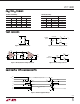
CMOS Output Driver
The LTC1480 transceiver provides full RS485 compatibility
while operating from a single 3.3V supply. The RS485
specification requires that a transceiver withstand common
mode voltages of up to 12V or –7V at the RS485 line
connections. Additionally, the transceiver must be immune
to both ESD and latch-up. This rules out traditional CMOS
drivers, which include parasitic diodes from their driver
outputs to each supply rail (Figure 9). The LTC1480 uses a
proprietary process enhancement which adds a pair of
Schottky diodes to the output stage (Figure 10), preventing
Figure 9. Conventional
CMOS Output Stage
Figure 10.
LTC1480 Output Stage
Figure 6. Driver Enable and Disable Times
Figure 7. Receiver Propagation Delays
Figure 8. Receiver Enable and Disable Times