
Datasheet
3
LTC1481
1481fa
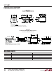
SYMBOL PARAMETER CONDITIONS MIN TYP MAX UNITS
t
PLH
Driver Input to Output R
DIFF
= 54Ω, C
L1
= C
L2
= 100pF, ● 10 30 60 ns
t
PHL
Driver Input to Output ● 10 30 60 ns
t
SKEW
Driver Output to Output ● 510ns
t
r
, t
f
Driver Rise or Fall Time ● 31540ns
t
ZH
Driver Enable to Output High C
L
= 100pF (Figures 4, 6), S2 Closed ● 40 70 ns
t
ZL
Driver Enable to Output Low C
L
= 100pF (Figures 4, 6), S1 Closed ● 40 70 ns
t
LZ
Driver Disable Time from Low C
L
= 15pF (Figures 4, 6), S1 Closed ● 40 70 ns
t
HZ
Driver Disable Time from High C
L
= 15pF (Figures 4, 6), S2 Closed ● 40 70 ns
t
PLH
Receiver Input to Output R
DIFF
= 54Ω, C
L1
= C
L2
= 100pF, ● 30 140 200 ns
t
PHL
Receiver Input to Output ● 30 140 200 ns
t
SKD
t
PLH
– t
PHL
Differential Receiver Skew ● 13 ns
t
ZL
Receiver Enable to Output Low C
RL
= 15pF (Figures 2, 8), S1 Closed ● 20 50 ns
t
ZH
Receiver Enable to Output High C
RL
= 15pF (Figures 2, 8), S2 Closed ● 20 50 ns
t
LZ
Receiver Disable from Low C
RL
= 15pF (Figures 2, 8), S1 Closed ● 20 50 ns
t
HZ
Receiver Disable from High C
RL
= 15pF (Figures 2, 8), S2 Closed ● 20 50 ns
f
MAX
Maximum Data Rate ● 2.5 Mbits/s
t
SHDN
Time to Shutdown DE = 0, RE = ● 50 200 600 ns
t
ZH(SHDN)
Driver Enable from Shutdown to Output High C
L
= 100pF (Figures 4, 6), S2 Closed ● 40 100 ns
t
ZL(SHDN)
Driver Enable from Shutdown to Output Low C
L
= 100pF (Figures 4, 6), S1 Closed ● 40 100 ns
t
ZH(SHDN)
Receiver Enable from Shutdown to Output High C
L
= 15pF (Figures 2, 8), S2 Closed ● 3500 ns
t
ZL(SHDN)
Receiver Enable from Shutdown to Output Low C
L
= 15pF (Figures 2, 8), S1 Closed ● 3500 ns
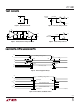
(Figures 3, 5)
(Figures 3, 7)
Note 1: Absolute Maximum Ratings are those values beyond which the life
of the device may be impaired.
Note 2: All currents into device pins are positive; all currents out of device
pins are negative. All voltages are referenced to device ground unless
otherwise specified.
Note 3: All typicals are given for V
CC
= 5V and T
A
= 25°C.
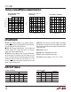
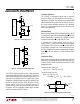
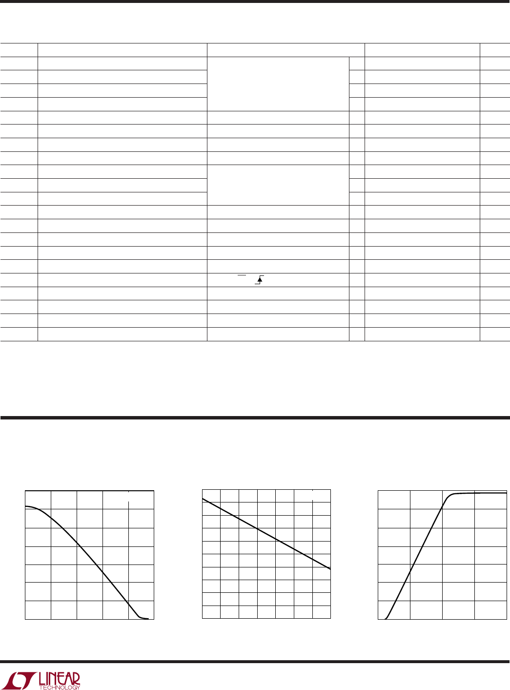
OUTPUT VOLTAGE (V)
0
70
60
50
40
30
20
10
0
3
1481 G01
12 45
OUTPUT CURRENT (mA)
T
A
= 25°C
Driver Differential Output Voltage
vs Output Current
TEMPERATURE (°C)
–50
DIFFERENTIAL VOLTAGE (V)
2.5
2.4
2.3
2.2
2.1
2.0
1.9
1.8
1.7
1.6
1.5
0
50
75
1481 G02
–25
25
100
125
R
L
= 54Ω
Driver Differential Output Voltage
vs Temperature
Driver Output Low Voltage
vs Output Current
OUTPUT VOLTAGE (V)
10
70
60
50
40
30
20
10
0
4
1481 G03
23
OUTPUT CURRENT (mA)
T
A
= 25°C
The ● denotes the specifications which apply over the full operating
temperature range, otherwise specifications are at T
A
= 25°C. V
CC
= 5V (Notes 2, 3) unless otherwise noted.
SWITCHI G CHARACTERISTICS
U
TYPICAL PERFOR A CE CHARACTERISTICS
UW