
Datasheet

4
LTC1481
1481fa
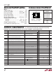
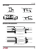
Driver Output High Voltage
vs Output Current
OUTPUT VOLTAGE (V)
0
OUTPUT CURRENT (mA)
4
5
0
–10
–20
–30
–40
–50
–60
–70
–80
–90
1481 G04
123
T
A
= 25°C
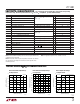
TEMPERATURE (°C)
–50
3.0
2.5
2.0
1.5
1.0
0.5
0
25 75
1481 G05
–25 0
50 100 125
TIME (ns)
TEMPERATURE (°C)
–50
14
12
10
8
6
4
2
0
25 75
1481 G05
–25 0
50 100 125
TIME (ns)
Driver Skew vs Temperature
Receiver t
PLH
– t
PHL
vs
Temperature
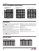
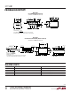
LTC1481 Transmitting
INPUTS OUTPUTS
RE DE DI B A
X1101
X1010
00XZZ
1 0 X Z* Z*
*Shutdown mode for LTC1481
LTC1481 Receiving
INPUTS OUTPUTS
RE DE A – B RO
00≥0.2V 1
00≤–0.2V 0
0 0 Inputs Open 1
10 X Z*
*Shutdown mode for LTC1481
DI (Pin 4): Driver Input. If the driver outputs are enabled
(DE high) then a low on DI forces the outputs A low and B
high. A high on DI with the driver outputs enabled will force
A high and B low.
GND (Pin 5): Ground.
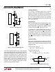
A (Pin 6): Driver Output/Receiver Input.
B (Pin 7): Driver Output/Receiver Input.
V
CC
(Pin 8): Positive Supply. 4.75V < V
CC
< 5.25V.
RO (Pin 1): Receiver Output. If the receiver output is
enabled (RE low), then if A > B by 200mV, RO will be high.
If A < B by 200mV, then RO will be low.
RE (Pin 2): Receiver Output Enable. A low enables the
receiver output, RO. A high input forces the receiver
output into a high impedance state.
DE (Pin 3): Driver Outputs Enable. A high on DE enables
the driver output. A, B and the chip will function as a line
driver. A low input will force the driver outputs into a high
impedance state and the chip will function as a line
receiver. If RE is high and DE is low, the part will enter a low
power (1µA) shutdown state.
TYPICAL PERFOR A CE CHARACTERISTICS
UW
UU
U
PI FU CTIO S
FU CTIO TABLES
U
U