
Datasheet
6
LTC1481
1481fa
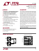
1.5V
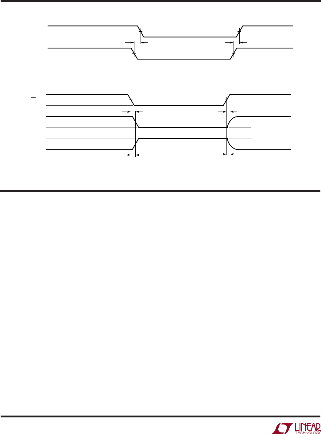
t
ZL(SHDN)
, t
ZL
t
ZH(SHDN)
, t
ZH
1.5V
1.5V
1.5V
t
LZ
0.5V
0.5V
t
HZ
OUTPUT NORMALLY LOW
OUTPUT NORMALLY HIGH
3V
0V
RE
5V
0V
RO
RO
LTC1481 • F08
f = 1MHz, t
r
≤ 10ns, t
f
≤ 10ns
Basic Theory of Operation
Traditionally, RS485 transceivers have been designed
using bipolar technology because the common mode
range of the device must extend beyond the supplies and
the device must be immune to ESD damage and latch-up.
Unfortunately, most bipolar devices draw a large amount
of supply current, which is unacceptable for the numerous
applications that require low power consumption. The
LTC1481 is a CMOS RS485/RS422 transceiver which
features ultralow power consumption without sacrificing
ESD and latch-up immunity.
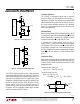
The LTC1481 uses a proprietary driver output stage,
which allows a common mode range that extends beyond
the power supplies while virtually eliminating latch-up and
providing excellent ESD protection. Figure 9 shows the
LTC1481 output stage while Figure 10 shows a conven-
tional CMOS output stage.
When the conventional CMOS output stage of Figure 10
enters a high impedance state, both the P-channel (P1)
and the N-channel (N1) are turned off. If the output is then
driven above V
CC
or below ground, the P+/N-well diode
(D1) or the N+/P-substrate diode (D2) respectively will
turn on and clamp the output to the supply. Thus, the
output stage is no longer in a high impedance state and is
not able to meet the RS485 common mode range require-
ment. In addition, the large amount of current flowing
through either diode will induce the well-known CMOS
latch-up condition, which could destroy the device.
The LTC1481 output stage of Figure 9 eliminates these
problems by adding two Schottky diodes, SD3 and SD4.
The Schottky diodes are fabricated by a proprietary modi-
fication to the standard N-well CMOS process. When the
output stage is operating normally, the Schottky diodes
are forward biased and have a small voltage drop across
them. When the output is in the high impedance state and
is driven above V
CC
or below ground, the parasitic diode
D1 or D2 still turns on, but SD3 or SD4 will reverse bias and
prevent current from flowing into the N-well or the sub-
strate. Thus the high impedance state is maintained even
with the output voltage beyond the supplies. With no
minority carrier current flowing into the N-well or sub-
strate, latch-up is virtually eliminated under power-up or
power-down conditions.
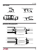
1.5V
t
PHL
RO
–V
OD2
A – B
0V 0V
1.5V
t
PLH
OUTPUT
INPUT
V
OD2
V
OL
V
OH
LTC1481 • F07
f = 1MHz, t
r
≤ 10ns, t
f
≤ 10ns
Figure 7. Receiver Propagation Delays
Figure 8. Receiver Enable and Disable Times
SWITCHI G TI E WAVEFOR S
UWW
APPLICATIO S I FOR ATIO
WUUU