
Datasheet

7
LTC1481
1481fa
Low Power Operation
The LTC1481 is designed to operate with a quiescent
current of 120µA max. With the driver in three-state, I
CC
will drop to this 120µA level. With the driver enabled there
will be additional current drawn by the internal 12k resis-
tor. Under normal operating conditions this additional
current is overshadowed by the current drawn by the
external bus impedance.
Shutdown Mode
Both the receiver output (RO) and the driver outputs (A, B)
can be placed in three-state mode by bringing RE high and
DE low respectively. In addition, the LTC1481 will enter
shutdown mode when RE is high and DE is low.
In shutdown the LTC1481 typically draws only 1µA of
supply current. In order to guarantee that the part goes
into shutdown, DE must be low and RE must be high for
at least 600ns simultaneously. If this time duration is less
than 50ns the part will not enter shutdown mode. Toggling
either RE or DE will wake the LTC1481 back up within
3.5µs.
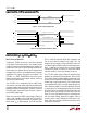
Propagation Delay
Many digital encoding schemes are dependent upon the
difference in the propagation delay times of the driver and
receiver. Figure 11 shows the test circuit for the LTC1481
propagation delay.
The receiver delay times are:
t
PLH
– t
PHL
= 13ns Typ, V
CC
= 5V
The drivers skew times are:
Skew = 5ns Typ, V
CC
= 5V
10ns Max, V
CC
= 5V, T
A
= –40°C to 85°C
Information furnished by Linear Technology Corporation is believed to be accurate and reliable.
However, no responsibility is assumed for its use. Linear Technology Corporation makes no represen-
tation that the interconnection of circuits as described herein will not infringe on existing patent rights.
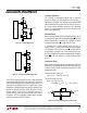
D
R
RECEIVER
OUT
R
54Ω
100pF
100pF
TTL IN
t
r
, t
f
< 6ns
LTC1481 • F11
Figure 11. Receiver Propagation Delay Test Circuit
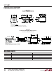
LOGIC
V
CC
SD3
P1
D1
OUTPUT
SD4
D2
N1
LTC1481 • F09
ESD
LOGIC
V
CC
P1
D1
OUTPUT
D2
N1
LTC1481 • F10
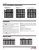
Figure 9. LTC1481 Output Stage
Figure 10. Conventional CMOS Output Stage
The LTC1481 output stage will maintain a high impedance
state until the breakdown of the N-channel or P-channel is
reached when going positive or negative respectively. The
output will be clamped to either V
CC
or ground by a Zener
voltage plus a Schottky diode drop, but this voltage is well
beyond the RS485 operating range. Because the ESD
injected current in the N-well or substrate consists of
majority carriers, latch-up is prevented by careful layout
techniques. An ESD cell protects output against multiple
10kV human body model ESD strikes.
APPLICATIO S I FOR ATIO
WUUU