
Datasheet

8
LTC1482
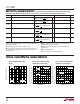
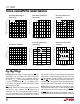
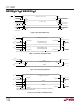
Driver Output High Voltage vs
Output Current
Driver Output Low Voltage vs
Output Current
Driver Propagation Delay vs
Temperature
Driver Skew vs Temperature
Driver Propagation Delay vs
Supply Voltage
Driver Short-Circuit Current vs
Temperature
TYPICAL PERFOR A CE CHARACTERISTICS
UW
TEMPERATURE (°C)
–55
DRIVER SHORT-CIRCUIT CURRENT (mA)
1482 G36
250
200
150
100
50
0
V
CC
= 5.25V
DRIVER OUTPUT HIGH
SHORT TO –7V
DRIVER OUTPUT LOW
SHORT TO 10V
–35 –15 5 25 45 65 85 105 125
TEMPERATURE (°C)
–55
DRIVER SKEW (ns)
1482 G34
5.0
4.5
4.0
3.5
3.0
2.5
2.0
1.5
1.0
0.5
0
–35 –15 5 25 45 65 85 105 125
SUPPLY VOLTAGE (V)
4.5
4.75 5 5.25 5.5
DRIVER PROPAGATION DELAY (ns)
1482 G35
40
35
30
25
20
15
10
5
0
T
A
= 25°C
t
PLH
t
PHL
TEMPERATURE (°C)
–55
DRIVER PROPAGATION DELAY (ns)
1482 G33
40
35
30
25
20
15
10
5
0
V
CC
= 5V
t
PHL
t
PLH
–35 –15 5 25 45 65 85 105 125
external (DE = 0) driver. A weak internal pull-up removes
the need for an external pull-up resistor if fast rise times
are not important. Several LTC1482s can share the same
CD line. CD = 1 forces RO to the high fail-safe state. In
shutdown, CD is three-stated. This pin can be pulled above
V
CC
but should not be taken above 8V to avoid damage.
DE (Pin 3): Driver Enable Input. DE = 0 disables or three-
states the driver outputs. DE = 1 enables the driver outputs
with the high/low state of the outputs set by DI/SHDN.
DI/SHDN (Pin 4): Driver Input and Shutdown Input. It is
used together with the DE pin to put the part in shutdown
PIN FUNCTIONS
UUU
RO (Pin 1): Receiver Output. If a carrier is present (CD low)
and the part is not in shutdown, RO is high if the receiver
input differential voltage (A – B) ≥ V
THRO(MAX)
and low if
(A – B) ≤ V
THRO(MIN)
. RO is forced to high (fail-safe state)
if a carrier is not present (CD = 1). In shutdown, RO is
three-stated. If the driver is enabled, RO follows the logic
level at the driver input.
CD (Pin 2): Open-Drain Carrier Detect Output. Provided
that the part is not in shutdown, the CD output is low if
V
THCD(MIN)
≥ (A – B) ≥ V
THCD(MAX)
and high if V
THCD(MIN)
< (A – B) < V
THCD(MAX)
. This is true regardless of whether
the A and B pins are driven by the internal (DE = 1) or an
OUTPUT CURRENT (mA)
0
10 20 30 40 50 60 70 80 90 100
DRIVER OUTPUT LOW VOLTAGE (V)
1482 G32
3.0
2.5
2.0
1.5
1.0
0.5
0
V
CC
= 4.75V
OUTPUT CURRENT (mA)
–100
–90 –80 –70 –60 –50 –40 –30 –20 –10 0
DRIVER OUTPUT HIGH VOLTAGE (V)
1482 G31
5.0
4.5
4.0
3.5
3.0
2.5
2.0
1.5
1.0
0.5
0
V
CC
= 4.75V