
Datasheet


6
LTC1483
sn1483 1483fs
SWITCHI G TI E WAVEFOR S
UW W
1.5V
t
PHL
RO
–V
OD2
A – B
0V 0V
1.5V
t
PLH
OUTPUT
INPUT
V
OD2
V
OL
V
OH
LTC1483 • F07
t
r
≤ 10ns, t
f
≤ 10ns
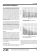
Figure 7. Receiver Propagation Delays
1.5V
t
ZL(SHDN)
, t
ZL
t
ZH(SHDN)
, t
ZH
1.5V
1.5V
1.5V
t
LZ
0.5V
0.5V
t
HZ
OUTPUT NORMALLY LOW
OUTPUT NORMALLY HIGH
3V
0V
RE
5V
0V
RO
RO
LTC1483 • F08
t
r
≤ 10ns, t
f
≤ 10ns
Figure 8. Receiver Enable and Disable Times
APPLICATIO S I FOR ATIO
UU W U
Basic Theory of Operation
Traditionally RS485 transceivers have been designed us-
ing bipolar technology because the common-mode range
of the device must extend beyond the supplies and the
device must be immune to ESD damage and latch-up.
Unfortunately, most bipolar devices draw a large amount
of supply current, which is unacceptable for the numerous
applications that require low power consumption. The
LTC1483 is a CMOS RS485/RS422 transceiver which
features ultra-low power consumption without sacrificing
ESD and latch-up immunity.
The LTC1483 uses a proprietary driver output stage,
which allows a common-mode range that extends beyond
the power supplies while virtually eliminating latch-up and
providing excellent ESD protection. Figure 9 shows the
LTC1483 output stage while Figure 10 shows a conven-
tional CMOS output stage.
When the conventional CMOS output stage of Figure 10
enters a high impedance state, both the P-channel (P1)
and the N-channel (N1) are turned off. If the output is then
driven above V
CC
or below ground, the P+/N-well diode
(D1) or the N+/P-substrate diode (D2) respectively will
turn on and clamp the output to the supply. Thus, the
output stage is no longer in a high impedance state and is
not able to meet the RS485 common-mode range require-
ment. In addition, the large amount of current flowing
through either diode will induce the well-known CMOS
latch-up condition, which could destroy the device.
LOGIC
V
CC
SD3
P1
D1
OUTPUT
SD4
D2
N1
LTC1483 • F09
Figure 9. LTC1483 Output Stage
LOGIC
V
CC
P1
D1
OUTPUT
D2
N1
LTC1483 • F10
Figure 10. Conventional
CMOS Output Stage