
Datasheet


7
LTC1483
sn1483 1483fs
APPLICATIO S I FOR ATIO
UU W U
The LTC1483 output stage of Figure 9 eliminates these
problems by adding two Schottky diodes, SD3 and SD4.
The Schottky diodes are fabricated by a proprietary modi-
fication to the standard N-well CMOS process. When the
output stage is operating normally, the Schottky diodes
are forward biased and have a small voltage drop across
them. When the output is in the high impedance state and
is driven above V
CC
or below ground, the parasitic diode
D1 or D2 still turns on, but SD3 or SD4 will reverse bias and
prevent current from flowing into the N-well or the sub-
strate. Thus the high impedance state is maintained even
with the output voltage beyond the supplies. With no
minority carrier current flowing into the N-well or sub-
strate, latch-up is virtually eliminated under power-up or
power-down conditions.
The LTC1483 output stage will maintain a high impedance
state until the breakdown of the N-channel or P-channel is
reached when going positive or negative respectively. The
output will be clamped to either V
CC
or ground by a Zener
voltage plus a Schottky diode drop, but this voltage is well
beyond the RS485 operating range. An ESD cell protects
output against multiple ±10kV human body model ESD
strikes. Because the ESD injected current in the N-well or
substrate consists of majority carriers, latch-up is pre-
vented by careful layout techniques.
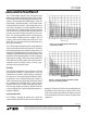
Slew Rate
The LTC1483 is designed for systems that are sensitive to
electromagnetic radiation. The part features a slew rate
limited driver that reduces high frequency electromag-
netic emissions, while improving signal fidelity by reduc-
ing reflections due to misterminated cables. Figures 11
and 12 show the spectrum of the signal at the driver output
for a standard slew rate RS485 driver and the slew rate
limited LTC1483. The LTC1483 shows significant reduc-
tion of the high frequency harmonics. Because the driver
is slew rate limited, the maximum operating frequency is
limited to 250kbits/s.
Low Power Operation
The LTC1483 is designed to operate with a quiescent
current of 120µA max. With the driver in three-state I
CC
will
Information furnished by Linear Technology Corporation is believed to be accurate and reliable.
However, no responsibility is assumed for its use. Linear Technology Corporation makes no represen-
tation that the interconnection of circuits as described herein will not infringe on existing patent rights.
0543
FREQUENCY (MHz)
21
20
10
0
–10
–20
–30
–40
–50
–60
–70
–80
LOG MAGNITUDE (dBV
RMS
)
05
4
3
FREQUENCY (MHz)
21
20
10
0
–10
–20
–30
–40
–50
–60
–70
–80
LOG MAGNITUDE (dBV
RMS
)
drop to this 120µA level. With the driver enabled there will
be additional current drawn by the internal 12k resistor.
Under normal operating conditions this additional current
is overshadowed by the current drawn by the external bus
impedance.
Figure 12. Slew Rate Limited LTC1483 Driver Output
Spectrum Transmitting at 150kHz
Figure 11. Typical RS485 Driver Output Spectrum
Transmitting at 150kHz