
Datasheet


11
LTC1484
APPLICATIONS INFORMATION
WUU
U
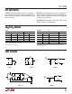
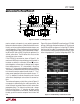
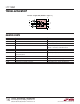
SWITCHI G TI E WAVEFOR S
UWW
1.5V
1.5V
NOTE: DI = 0, RE = 0, A AND B ARE THREE-STATED WHEN DE = 0
t
DZR
OUTPUT NORMALLY LOW
OUTPUT NORMALLY HIGH
3V
0V
DE
V(A) – V(B)
RO
1484 F10
f = 1MHz, t
r
≤ 10ns, t
f
≤ 10ns
Figure 10. Driver Enable to Receiver Valid Timing
Low Power Operation
The LTC1484 has a quiescent current of 900µA max when
the driver is enabled. With the driver in three-state, the
supply current drops to 700µA max. The difference in
these supply currents is due to the additional current
drawn by the internal 22k receiver input resistors when the
driver is enabled. Under normal operating conditions, the
additional current is overshadowed by the 50mA current
drawn by the external termination resistor.
Receiver Open-Circuit Fail-Safe
Some encoding schemes require that the output of the
receiver maintain a known state (usually a logic 1) when
data transmission ends and all drivers on the line are
forced into three-state. Earlier RS485 receivers with a
weak pull-up at the A input will give a high output only
when the inputs are floated. When terminated or shorted
together, the weak pull-up is easily defeated causing the
receiver output to go low. External components are needed
if a high receiver output is mandatory. The receiver of the
LTC1484 has a fail-safe feature which guarantees the
output to be in a logic 1 when the receiver inputs are left
open or shorted together, regardless of whether the termi-
nation resistor is present or not.
In encoding schemes where the required known state is a
low, external components are needed for the LTC1484 and
other RS485 parts.
Fail-safe is achieved by making the receiver trip points fall
within the V
TH(MIN)
to V
TH(MAX)
range. When any of the
listed receiver input conditions exist, the receiver inputs
are effectively at 0V and the receiver output goes high.
The receiver fail-safe mechanism is designed to reject fast
common mode steps (–7V to 12V in 10ns) switching at
100kHz typ. This is achieved through an internal carrier
detect circuit similar to the LTC1482. This circuit has built-
in delays to prevent glitches while the input swings be-
tween ±V
TH(MAX)
levels. When all the drivers connected to
the receiver inputs are three-stated, the internal carrier
detect signal goes low to indicate that no differential signal
is present. When any driver is taken out of three-state, the
carrier detect signal takes 1.6µs typ (see t
DZR
) to detect the
enabled driver. During this interval, the transceiver output
(RO) is forced to the fail-safe high state. After 1.6µs, the
receiver will respond normally to changes in driver output.
If the part is taken out of shutdown mode with the receiver
inputs floating, the receiver output takes about 10µs to
leave three-state (see t
ZL(SHDN)
). If the receiver inputs are
actively driven to a high state, the outputs go high after
about 5.5µs.