
Datasheet


4
LTC1484
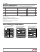
SYMBOL PARAMETER CONDITIONS MIN TYP MAX UNITS
t
ZH(SHDN)
Driver Enable from Shutdown to Output High C
L
= 100pF (Figures 5, 7) S2 Closed, ● 40 100 ns
DI = DE
t
ZL(SHDN)
Driver Enable from Shutdown to Output Low C
L
= 100pF (Figures 5, 7) S1 Closed, ● 40 100 ns
DI = 0
t
ZH(SHDN)
Receiver Enable from Shutdown to Output High C
L
= 15pF (Figures 3, 9) S2 Closed, ● 10 µs
DE = 0
t
ZL(SHDN)
Receiver Enable from Shutdown to Output Low C
L
= 15pF (Figures 3, 9) S1 Closed, ● 10 µs
DE = 0
Note 1: Absolute Maximum Ratings are those values beyond which the life of
a device may be impaired.
Note 2: All typicals are given for V
CC
= 5V and T
A
= 25°C.
Note 3: All currents into device pins are positive; all currents out of device
pins are negative. All voltages are referenced to device ground unless
otherwise specified.
Note 4: For higher ambient temperatures, the part may enter thermal
shutdown during short-circuit conditions.
Note 5: Guaranteed by design.
Note 6: Time for I
CC
to drop to I
CC
/2 when the receiver is disabled.
SWITCHING CHARACTERISTICS
U
The ● denotes the specifications which apply over the full operating
temperature range, otherwise specifications are at T
A
= 25°C. V
CC
= 5V ±5% (Notes 2 and 3) unless otherwise noted.
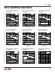
TYPICAL PERFOR A CE CHARACTERISTICS
UW
INPUT VOLTAGE (V)
–0.2
–0.16 –0.12 –0.08 –0.04 0
RECEIVER OUTPUT VOLTAGE (V)
1484 G01
6
5
4
3
2
1
0
T
A
= 25°C
V
CC
= 5V
V
TH(HIGH)
V
TH(LOW)
TEMPERATURE (°C)
–55 –35 –15 5 25 45 65 85 105 125
RECEIVER INPUT THRESHOLD VOLTAGE (V)
1484 G02
0
–0.05
–0.10
–0.15
–0.20
–0.25
V
CC
= 5V
V
TH(HIGH)
V
CM
= –7V
V
CM
= 12V
V
CM
= 0V
TEMPERATURE (°C)
–55 –35 –15 5 25 45 65 85 105 125
RECEIVER INPUT THRESHOLD VOLTAGE (V)
1484 G03
0
–0.05
–0.10
–0.15
–0.20
–0.25
V
CC
= 5V
V
TH(LOW)
V
CM
= –7V
V
CM
= 12V
V
CM
= 0V
Receiver Output Voltage vs Input
Voltage
Receiver Input Threshold Voltage
(Output High) vs Temperature
Receiver Input Threshold Voltage
(Output Low) vs Temperature