
Datasheet


9
LTC1484
PIN FUNCTIONS
UUU
A (Pin 6): Driver Output/Receiver Input. The input resis-
tance is typically 22k when the driver is disabled (DE = 0).
When the driver is enabled, the A output follows the logic
level at the DI pin.
B (Pin 7): Driver Output/Receiver Input. The input resis-
tance is typically 22k when the driver is disabled (DE = 0).
When the driver is enabled, the B output is inverted from
the logic level at the DI pin.
V
CC
(Pin 8): Positive Supply. 4.75V ≤ V
CC
≤ 5.25V. A 0.1µF
bypass capacitor is recommended.
Driver
INPUTS OUTPUTS
RE DE DI B A
X1101
X1010
O0XZZ
10XZ*Z*
FU CTIO TABLES
U
U
Receiver
INPUTS OUTPUTS
RE DE A – B RO
00 ≥V
TH(MAX)
1
00 ≤V
TH(MIN)
0
0 0 Inputs Open 1
0 0 Inputs Shorted 1
1X X Z
†
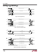
TEST CIRCUITS
OUTPUT
UNDER
TEST
C
L
S1
S2
V
CC
500Ω
1484 F05
OUTPUT
UNDER
TEST
C
RL
1k
S1
S2
V
CC
1k
1484 F03
Figure 3
Figure 5
DE
RE
A
B
DI
C
L1
R
DIFF
C
L2
RO
15pF
A
B
1484 F04
Figure 4
Note: Z = high impedance, X = don’t care
*Shutdown mode for LTC1484
†
Shutdown mode for LTC1484 if DE = 0. Table valid with or without
termination resistors.
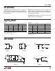
V
OD1
V
OD2
A
B
R
R
V
OC
1484 F01
Figure 1
V
OD3
A
B
375Ω
375Ω
60Ω
–7V TO 12V
1484 F02
Figure 2