
Datasheet

14
LTC1484
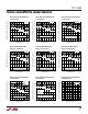
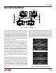
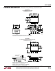
longer delay for the falling edge is due to the larger voltage
range the line must swing (typically >2V compared to
370mV) before the receiver trips high again. The differ-
ence in delay affects the duty cycle of the received data and
depends on cable capacitance. For a 1-foot STP cable, the
delays drop to 0.13µs and 0.4µs. Using smaller valued
pull-up and pull-down resistors to equalize the positive
and negative voltage swings needed to trip the receivers
will reduce the difference in delay and increase the maxi-
mum data rate. With 220Ω resistors, both rising and
falling edge delays are 2.2µs when driving a 1000-foot STP
cable as shown in Figure 12b.
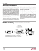
The fail-safe feature of the LTC1484 receiver allows a
CDMA system to function without the A and B pull-up and
pull-down resistors. However, if the resistors are left out,
noise margin will be reduced to as low as 15mV and
propagation delays will increase significantly. Operation in
this mode is not recommended.
Since DE and RE are tied together, the part never shuts
down. The receiver inputs are never floating (due to the
external bias resistors) so that the t
DZR
timing does not
apply to this application. The whole system can be changed
to actively transmit only a “1” by swapping the pull-up and
pull-down resistors in Figure 11, shorting DI to V
CC
and
connecting the 1k resistor as a pull-down. In this configu-
ration the driver is noninverting and the receiver output RO
truly follows DE.
APPLICATIONS INFORMATION
WUU
U
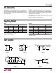
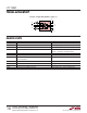
PACKAGE DESCRIPTION
U
Dimensions in inches (millimeters), unless otherwise noted.
MS8 Package
8-Lead Plastic MSOP
(LTC DWG # 05-08-1660)
MSOP (MS8) 1098
* DIMENSION DOES NOT INCLUDE MOLD FLASH, PROTRUSIONS OR GATE BURRS. MOLD FLASH,
PROTRUSIONS OR GATE BURRS SHALL NOT EXCEED 0.006" (0.152mm) PER SIDE
** DIMENSION DOES NOT INCLUDE INTERLEAD FLASH OR PROTRUSIONS.
INTERLEAD FLASH OR PROTRUSIONS SHALL NOT EXCEED 0.006" (0.152mm) PER SIDE
0.021
± 0.006
(0.53 ± 0.015)
0
° – 6° TYP
SEATING
PLANE
0.007
(0.18)
0.040
± 0.006
(1.02 ± 0.15)
0.012
(0.30)
REF
0.006 ± 0.004
(0.15 ± 0.102)
0.034 ± 0.004
(0.86 ± 0.102)
0.0256
(0.65)
BSC
12
3
4
0.193 ± 0.006
(4.90 ± 0.15)
8
7
6
5
0.118 ± 0.004*
(3.00 ± 0.102)
0.118 ± 0.004**
(3.00 ± 0.102)