
Datasheet

2
LTC1484
ABSOLUTE MAXIMUM RATINGS
W
WW
U
(Note 1)
Supply Voltage (V
CC
)............................................... 6.5V
Control Input Voltages ................. –0.3V to (V
CC
+ 0.3V)
Driver Input Voltage ..................... –0.3V to (V
CC
+ 0.3V)
Driver Output Voltages ................................. –7V to 10V
Receiver Input Voltages (Driver Disabled) .. –12V to 14V
Receiver Output Voltage............... –0.3V to (V
CC
+ 0.3V)
Junction Temperature .......................................... 125°C
Operating Temperature Range
LTC1484C .........................................0°C ≤ T
A
≤ 70°C
LTC1484I...................................... –40°C ≤ T
A
≤ 85°C
Storage Temperature Range ................. –65°C to 150°C
Lead Temperature (Soldering, 10 sec).................. 300°C
The ● denotes the specifications which apply over the full operating
temperature range, otherwise specifications are at T
A
= 25°C. V
CC
= 5V ±5% (Notes 2 and 3) unless otherwise noted.
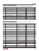
SYMBOL PARAMETER CONDITIONS MIN TYP MAX UNITS
V
OD1
Differential Driver Output Voltage (Unloaded) I
OUT
= 0 ● V
CC
V
V
OD2
Differential Driver Output Voltage (with Load) R = 50Ω (RS422) ● 2V
R = 27Ω (RS485) Figure 1
● 1.5 5 V
R = 22Ω, Figure 1
● 1.5 5 V
V
OD3
Differential Driver Output Voltage V
TST
= –7V to 12V, Figure 2 ● 1.5 5 V
(with Common Mode)
∆V
OD
Change in Magnitude of Driver Differential R = 22Ω, 27Ω or R = 50Ω, Figure 1 ● 0.2 V
Output Voltage for Complementary Output States V
TST
= –7V to 12V, Figure 2
V
OC
Driver Common Mode Output Voltage R = 22Ω, 27Ω or R = 50Ω, Figure 1 ● 3V
∆|V
OC
| Change in Magnitude of Driver Common Mode R = 22Ω, 27Ω or R = 50Ω, Figure 1 ● 0.2 V
Output Voltage for Complementary Output States
V
IH
Input High Voltage DE, DI, RE ● 2.0 V
V
IL
Input Low Voltage DE, DI, RE ● 0.8 V
I
IN1
Input Current DE, DI, RE ● ±2 µA
I
IN2
Input Current (A, B) DE = 0, V
CC
= 0 or 5V, V
IN
= 12V ● 1.0 mA
DE = 0, V
CC
= 0 or 5V, V
IN
= –7V ● –0.8 mA
V
TH
Differential Input Threshold Voltage for Receiver –7V ≤ V
CM
≤ 12V, DE = 0 ● –0.20 –0.015 V
ELECTRICAL CHARACTERISTICS
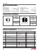
PACKAGE/ORDER INFORMATION
W
U
U
ORDER PART
NUMBER
ORDER PART
NUMBER
LTC1484CMS8 LTC1484CN8
LTC1484CS8
LTC1484IN8
LTC1484IS8
S8 PART MARKING
1484
1484I
MS8 PART MARKING
LTDX
T
JMAX
= 125°C, θ
JA
= 200°C/ W
T
JMAX
= 125°C, θ
JA
= 130°C/ W (N8)
T
JMAX
= 125°C, θ
JA
= 135°C/W (S8)
Consult factory for Military grade parts.
1
2
3
4
RO
RE
DE
DI
8
7
6
5
V
CC
B
A
GND
TOP VIEW
MS8 PACKAGE
8-LEAD PLASTIC MSOP
1
2
3
4
8
7
6
5
TOP VIEW
RO
RE
DE
DI
V
CC
B
A
GND
N8 PACKAGE
8-LEAD PDIP
S8 PACKAGE
8-LEAD PLASTIC SO
R
D