
Datasheet

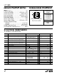


5
LTC1485
PI FU CTIO S
U
UU
RO (Pin 1): Receiver Output. If the receiver output is
enabled (RE low), then if A > B by 200mV, RO will be high.
If A < B by 200mV, then RO will be low.
RE (Pin 2): Receiver Output Enable. A low enables the
receiver output, RO. A high input forces the receiver
output into a high impedance state.
DE (Pin 3): Driver Output Enable. A high on DE enables the
driver outputs, A and B. A low input will force the driver
outputs into a high impedance state.
DI (Pin 4): Driver Input. If the driver outputs are enabled
(DE high), then a low on DI forces the driver outputs A low
and B high. A high on DI will force A high and B low.
GND (Pin 5): Ground Connection.
A (Pin 6): Driver Output/Receiver Input.
B (Pin 7): Driver Output/Receiver Input.
V
CC
(Pin 8): Positive Supply. 4.75V ≤ V
CC
≤ 5.25V.
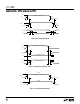
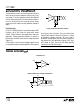
TEST CIRCUITS
Figure 3. Receiver Timing Test Load
1k
1485 F03
C
L
S1
S2
1k
V
CC
RECEIVER
OUTPUT
Figure 4. Driver Timing Test Load
1485 F04
C
L
S1
S2
500Ω
V
CC
OUTPUT
UNDER TEST
V
OD2
A
B
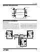
R
R
V
OC
1485 F01
DI R
DIFF
1485 F02
DRIVER RECEIVER
C
L1
C
L2
RO
15pF
A
B
A
B
Figure 1. Driver DC Test Load Figure 2. Driver/Receiver Timing Test Circuit