
Datasheet

2
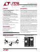
LTC1518/LTC1519
(Note 1)
Supply Voltage ....................................................... 10V
Digital Input Currents ..................... –100mA to 100mA
Digital Input Voltages ............................... –0.5V to 10V
Receiver Input Voltages ........................................ ±14V
Receiver Output Voltages ............. –0.5V to V
DD
+ 0.5V
Receiver Input Differential ....................................... 10V
Short-Circuit Duration .................................... Indefinite
Operating Temperature Range
LTC1518C/LTC1519C ............................. 0°C to 70°C
LTC1518I/LTC1519I .......................... –40°C to 85°C
Storage Temperature Range ................ –65°C to 150°C
Lead Temperature (Soldering, 10 sec)................. 300°C
T
JMAX
= 150°C, θ
JA
= 90°C/W
Consult factory for Military grade parts.
ORDER PART
NUMBER
LTC1518CS
LTC1518IS
ORDER PART
NUMBER
LTC1519CS
LTC1519IS
T
JMAX
= 150°C, θ
JA
= 90°C/W
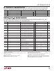
SYMBOL PARAMETER CONDITIONS MIN TYP MAX UNITS
V
CM
Input Common Mode Voltage A, B Inputs ● –7 12 V
V
IH
Input High Voltage EN, EN, EN12, EN34 ● 2V
V
IL
Input Low Voltage EN, EN, EN12, EN34 ● 0.8 V
I
IN1
Input Current EN, EN, EN12, EN34 ● –1 1 µA
I
IN2
Input Current (A, B) V
A
, V
B
= 12V ● 500 µA
V
A
, V
B
= –7V ● –500 µA
R
IN
Input Resistance –7V ≤ V
CM
≤ 12V (Figure 5) ● 22 kΩ
C
IN
Input Capacitance (Note 4) 3 pF
V
OC
Open-Circuit Input Voltage V
DD
= 5V (Note 4) (Figure 5) ● 3.2 3.3 3.4 V
V
ID(MIN)
Differential Input Threshold Voltage –7V ≤ V
CM
≤ 12V ● –0.3 0.3 V
dV
ID
Input Hysteresis V
CM
= 2.5V 25 mV
V
OH
Output High Voltage I
OUT
= –4mA, V
ID
= 0.3V, V
DD
= 5V ● 4.6 V
V
OL
Output Low Voltage I
OUT
= 4mA, V
ID
= –0.3V, V
DD
= 5V ● 0.4 V
I
OZR
Three-State Output Current 0V < V
OUT
< 5V ● –10 10 µA
I
DD
Total Supply Current All 4 Receivers V
ID
> 0.3V, No Load, Device Enabled ● 12 20 mA
I
OSR
Short-Circuit Current V
OUT
= 0V, V
OUT
= 5V (Note 7) ● –50 50 mA
The ● denotes specifications which apply over the full operating
temperature range, otherwise specifications are at T
A
= 25°C. V
DD
= 5V ±5% (Notes 2, 3) per receiver, unless otherwise noted.
ABSOLUTE AXI U RATI GS
WWWU
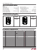
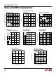
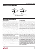
PACKAGE/ORDER I FOR ATIO
UU
W
TOP VIEW
S PACKAGE
16-LEAD PLASTIC SO
1
2
3
4
5
6
7
8
16
15
14
13
12
11
10
9
B1
A1
OUT 1
EN
OUT 2
A2
B2
GND
V
DD
B4
A4
OUT 4
EN
OUT 3
A3
B3
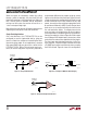
TOP VIEW
S PACKAGE
16-LEAD PLASTIC SO
1
2
3
4
5
6
7
8
16
15
14
13
12
11
10
9
B1
A1
OUT 1
EN12
OUT 2
A2
B2
GND
V
DD
B4
A4
OUT 4
EN34
OUT 3
A3
B3
DC ELECTRICAL CHARACTERISTICS