
Datasheet

7
LTC1518/LTC1519
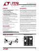
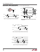
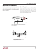
Figure 5. Input Thevenin Equivalent
Theory of Operation
Unlike typical line receivers whose propagation delay can
vary by as much as 500% from package to package and
show significant temperature drift, the LTC1518/LTC1519
employ a novel architecture that produces a tightly con-
trolled and temperature compensated propagation delay.
The differential timing skew is also minimized between
rising and falling output edges, and the propagation delays
of any two receivers within a package are very tightly
matched.
The precision timing features of the LTC1518/LTC1519
reduce overall system timing constraints by providing a
narrow ±3.5ns window during which valid data appears at
the receiver output. This output timing window applies to
all receivers in all packages over the commercial operating
temperature range, thereby making the LTC1518/LTC1519
well suited for high speed data transmission.
In clocked data systems, the low skew minimizes duty
cycle distortion of the clock signal. The LTC1518/LTC1519
can propagate signals at frequencies of 26MHz (52Mbps)
with less than 5% duty cycle distortion. When a clock
signal is used to retime parallel data, the maximum recom-
mended data transmission rate is 25Mbps to avoid timing
errors due to clock distortion.
Thermal shutdown and short-circuit protection prevent
latchup damage to the LTC1518/LTC1519 during fault
conditions.
Fail-Safe Features
The LTC1518/LTC1519 have a fail-safe feature that guar-
antees the output to be in a logic HIGH state when the
inputs are either shorted or left open (note that when
inputs are left open, any external large leakage current
might override the fail-safe). The fail-safe feature detects
shorted inputs over the entire common mode range. When
a fault is detected, the output will typically go high in 2µs.
When some of the receivers within a package are not
used, the open fail-safe feature will allow the user to let
the receiver inputs float and maintain a high logic state at
the output. Without the open fail-safe feature, any noise
at the input would cause unwanted glitches at the output.
When the inputs are left “open,” one must make sure that
there are no sources of leakage current connected to one
or both of the inputs. This can happen if the device is
being driven single-endedly and both the signal and the
DC bias are disconnected. If the capacitor used to bypass
the DC bias is left connected to the input of the device and
is leaky (>1µA), the output of the device might not be the
desired high logic state. Also keep in mind that the inputs
are high impedance (≥22kΩ). When left open, noisy
traces should be kept away from the receiver inputs to
minimize capacitive coupling of undesired signals. Even
with the open fail-safe feature, for maximum noise
immunity, grounding the negative input of unused re-
ceivers is recommended.
EQUIVALE T I PUT NETWORKS
UU
3.3V
≥22k
≥22k
A
B
RECEIVER ENABLED, V
DD
= 5V RECEIVER DISABLED OR V
DD
= 0V
3.3V
≥22k
A
B
1518/19 F05
≥22k
APPLICATIO S I FOR ATIO
WUUU