
Datasheet
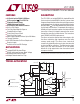

LTC1535
4
1535fb
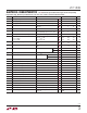
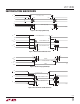
ELECTRICAL CHARACTERISTICS
SYMBOL PARAMETER CONDITIONS MIN TYP MAX UNITS
t
SJ
Data Sample Jitter Figure 8, (Note 7)
l
250 285 ns
f
MAX
Max Baud Rate Jitter = 10% Max, SLO = 1, (Note 8)
l
250 410 kBd
t
PLH
Driver Input to Output DE = 1, SLO = 1, Figure 4, Figure 6
DE = 1, SLO = 0, Figure 4, Figure 6
l
l
600
1300
855
1560
ns
ns
t
PHL
Driver Input to Output DE = 1, SLO = 1, Figure 4, Figure 6
DE = 1, SLO = 1, Figure 4, Figure 6
l
l
600
1300
855
1560
ns
ns
t
r
, t
f
Driver Rise or Fall Time DE = 1, SLO = 1, Figure 4, Figure 6
DE = 1, SLO = 0, V
CC
= V
CC2
= 4.5V
l
l
150
20
500
100
1000
ns
ns
t
ZH
Driver Enable to Output DI = 1, SLO = 1, Figure 5, Figure 7
l
1000 1400 ns
t
ZL
Driver Enable to Output DI = 0, SLO = 1, Figure 5, Figure 7
l
1000 1400 ns
t
LZ
Driver Disable to Output DI = 0, SLO = 1, Figure 5, Figure 7
l
700 1300 ns
t
HZ
Driver Disable to Output DI = 1, SLO = 1, Figure 5, Figure 7
l
700 1300 ns
t
PLH
Receiver Input to RO RE = 0, Figure 3, Figure 8
l
600 855 ns
t
PHL
Receiver Input to RO RE = 0, Figure 3, Figure 8
l
600 855 ns
t
PLH
Receiver Input to RO2 RE = 0, Figure 3, Figure 8 30 ns
t
PHL
Receiver Input to RO2 RE = 0, Figure 3, Figure 8 30 ns
t
r
, t
f
Receiver Rise or Fall Time RE = 0, Figure 3, Figure 8 20 ns
t
LZ
Receiver Disable to Output Figure 3, Figure 9 30 ns
t
HZ
Receiver Disable to Output Figure 3, Figure 9 30 ns
t
START
Initial Start-Up Time (Note 9) 1200 ns
t
TOF
Data Time-Out Fault (Note 9) 1200 ns
ST1, ST2 Duty Cycle 0°C ≤ T
A
≤ 70°C
–40°C ≤ T
A
≤ 85°C
l
l
56
57
%
%
The l denotes the specifi cations which apply over the full operating
temperature range, otherwise specifi cations are at T
A
= 25°C. V
CC
= 5V, V
CC2
= 5V, R = 27Ω (RS485) unless otherwise noted.
Note 1: Absolute Maximum Ratings are those values beyond which the life
of a device may be impaired.
Note 2: RS422 50Ω specifi cation based on RS485 27Ω test.
Note 3: I
IN
is tested at V
CC2
= 5V, guaranteed by design from
GND2 ≤ V
CC2
≤ 5.25V.
Note 4: Input fault conditions on the RS485 receiver are detected with a
fi xed receiver offset. The offset is such that an input short or open will
result in a high data output.
Note 5: The low voltage detect faults when V
CC2
or V
CC
drops below
V
UVL
and reenables when greater than V
UVH
. The fault can be monitored
through the weak driver output on RE.
Note 6: Value derived from 1 second test.
Note 7: The input signals are internally sampled and encoded. The internal
sample rate determines the data output jitter since the internal sampling is
asynchronous with respect to the external data. Nominally, a 4MHz internal
sample rate gives 250ns of sampling uncertainty in the input signals.
Note 8: The maximum baud rate is 250kBd with 10% sampling jitter.
Lower baud rates have lower jitter.
Note 9: Start-up time is the time for communication to recover after a fault
condition. Data time-out is the time a fault is indicated on RE after data
communication has stopped.
Note 10: I
CC
measured with no load, ST1 and ST2 fl oating.