
Datasheet


5
LTC1544
V
CC
(Pin 1): Positive Supply for the Transceivers. 4.75V ≤
V
CC
≤ 5.25V. Connect a 1µF capacitor to ground.
V
DD
(Pin 2): Positive Supply Voltage for V.28. Connect to
V
DD
Pin 3 on LTC1543 or 8V supply. Connect a 1µF
capacitor to ground.
D1 (Pin 3): TTL Level Driver 1 Input.
D2 (Pin 4): TTL Level Driver 2 Input.
D3 (Pin 5): TTL Level Driver 3 Input.
R1 (Pin 6): CMOS Level Receiver 1 Output.
R2 (Pin 7): CMOS Level Receiver 2 Output.
R3 (Pin 8): CMOS Level Receiver 3 Output.
D4 (Pin 9): TTL Level Driver 4 Input.
R4 (Pin 10): CMOS Level Receiver 4 Output.
M0 (Pin 11): TTL Level Mode Select Input 0 with Pull-Up
to V
CC
.
M1 (Pin 12): TTL Level Mode Select Input 1 with Pull-Up
to V
CC
.
M2 (Pin 13): TTL Level Mode Select Input 2 with Pull-Up
to V
CC
.
DCE/DTE (Pin 14): TTL Level Mode Select Input with
Pull-Up to V
CC
.
INVERT (Pin 15): TTL Level Mode Select Input with Pull-
Up to V
CC
.
D4/R4 A (Pin 16): Receiver 4 Inverting Input and Driver 4
Output.
R3 B (Pin 17): Receiver 3 Noninverting Input.
R3 A (Pin 18): Receiver 3 Inverting Input.
R2 B (Pin 19): Receiver 2 Noninverting Input.
R2 A (Pin 20): Receiver 2 Inverting Input.
D3/R1 B (Pin 21): Receiver 1 Noninverting Input and
Driver 3 Noninverting Output.
D3/R1 A (Pin 22): Receiver 1 Inverting Input and Driver 3
Inverting Output.
D2 B (Pin 23): Driver 2 Noninverting Output.
D2 A (Pin 24): Driver 2 Inverting Output.
D1 B (Pin 25): Driver 1 Noninverting Output.
D1 A (Pin 26): Driver 1 Inverting Output.
GND (Pin 27): Ground.
V
EE
(Pin 28): Negative Supply Voltage. Connect to V
EE
Pin
26 on LTC1543 or to –8V supply. Connect a 1µF capacitor
to ground.
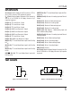
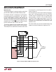
Figure 1. V.11 Driver Test Circuit
A
B
A
R
B
1544 F02
R
L
100Ω
C
L
100pF
C
L
100pF
15pF
A
B
1544 F01
V
OD
V
OC
R
L
50Ω
R
L
50Ω
Figure 2. V.11 Driver/Receiver AC Test Circuit
UU
U
PI FU CTIO S
TEST CIRCUITS