
Datasheet

4
LTC1544
Note 1: Absolute Maximum Ratings are those beyond which the safety of a
device may be impaired.
Note 2: All currents into device pins are positive; all currents out of device
are negative. All voltages are referenced to device ground unless otherwise
specified.
Note 3: All typicals are given for V
CC
= 5V, V
DD
= 8V, V
EE
= –7V for V.28,
–5.5V for V.10, V.11 and T
A
= 25°C.
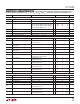
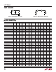
SYMBOL PARAMETER CONDITIONS MIN TYP MAX UNITS
V.10 Driver
V
O
Output Voltage Open Circuit, R
L
= 3.9k ● ±4 ±6V
V
T
Output Voltage R
L
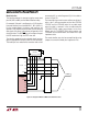
= 450Ω (Figure 3) ● ±3.6 V
R
L
= 450Ω (Figure 3) 0.9V
O
I
SS
Short-Circuit Current V
O
= GND ±150 mA
I
OZ
Output Leakage Current –0.25V ≤ V
O
≤ 0.25V, Power Off or ● ±0.1 ±100 µA
No-Cable Mode or Driver Disabled
t
r
, t
f
Rise or Fall Time R
L
= 450Ω, C
L
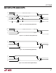
= 100pF (Figures 3, 7) 2 µs
t
PLH
Input to Output R
L
= 450Ω, C
L
= 100pF (Figures 3, 7) 1 µs
t
PHL
Input to Output R
L
= 450Ω, C
L
= 100pF (Figures 3, 7) 1 µs
V.10 Receiver
V
TH
Receiver Input Threshold Voltage ● –0.25 0.25 V
∆V
TH
Receiver Input Hysteresis ● 25 50 mV
I
IN
Receiver Input Current –10V ≤ V
A
≤ 10V ● ±0.66 mA
R
IN
Receiver Input Impedance –10V ≤ V
A
≤ 10V ● 15 30 kΩ
t
r
, t
f
Rise or Fall Time (Figures 4, 8) 15 ns
t
PLH
Input to Output (Figures 4, 8) 55 ns
t
PHL
Input to Output (Figures 4, 8) 109 ns
∆t Input to Output Difference, t
PLH
– t
PHL
(Figures 4, 8) 60 ns
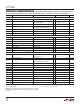
V.28 Driver
V
O
Output Voltage Open Circuit ● ±10 V
R
L
= 3k (Figure 3) ● ±5 ±8.5 V
I
SS
Short-Circuit Current V
O
= GND ● ±150 mA
I
OZ
Output Leakage Current –0.25V ≤ V
O
≤ 0.25V, Power Off or ● ±1 ±100 µA
No-Cable Mode or Driver Disabled
SR Slew Rate R
L
= 3k, C
L
= 2500pF (Figures 3, 7) ● 430V/µs
t
PLH
Input to Output R
L
= 3k, C
L
= 2500pF (Figures 3, 7) ● 1.3 2.5 µs
t
PHL
Input to Output R
L
= 3k, C
L
= 2500pF (Figures 3, 7) ● 1.3 2.5 µs
V.28 Receiver
V
THL
Input Low Threshold Voltage ● 1.5 0.8 V
V
TLH
Input High Threshold Voltage ● 2 1.6 V
∆V
TH
Receiver Input Hysterisis ● 0 0.1 0.3 V
R
IN
Receiver Input Impedance –15V ≤ V
A
≤ 15V ● 357 kΩ
t
r
, t
f
Rise or Fall Time (Figures 4, 8) 15 ns
t
PLH
Input to Output (Figures 4, 8) ● 60 100 ns
t
PHL
Input to Output (Figures 4, 8) ● 150 450 ns
The ● denotes specifications which apply over the full operating tempera-
ture range, otherwise specifications are at T
A
= 25°C. V
CC
= 5V, V
DD
= 8V, V
EE
= – 7V for V.28, – 5.5V for V.10, V.11 (Notes 2, 3)
ELECTRICAL CHARACTERISTICS