
Datasheet


4
LTC1629-6
16296f
ELECTRICAL CHARACTERISTICS
Note 4: Dynamic supply current is higher due to the gate charge being
delivered at the switching frequency. See Applications Information.
Note 5: The minimum on-time condition corresponds to the on inductor
peak-to-peak ripple current ≥40% of I
MAX
(see Minimum On-Time
Considerations in the Applications Information section).
Note 6: The LTC1629EG-6 is guaranteed to meet performance
specifications from 0°C to 70°C. Specifications over the –40°C to 85°C
operating temperature range are assured by design, characterization and
correlation with statistical process controls.
Note 1: Absolute Maximum Ratings are those values beyond which the
life of a device may be impaired.
Note 2: T
J
is calculated from the ambient temperature T
A
and power
dissipation P
D
according to the following formulas:
T
J
= T
A
+ (P
D
• 95°C/W)
Note 3: The I.C. is tested in a feedback loop that servos V
ITH
to a
specified voltage and measures the resultant V
EAIN
.
TYPICAL PERFOR A CE CHARACTERISTICS
UW
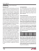
Efficiency vs Output Current
(Figure 12)
Efficiency vs Output Current
(Figure 12)
Efficiency vs Input Voltage
(Figure 12)
OUTPUT CURRENT (A)
0.1
EFFICIENCY (%)
100
80
60
40
20
0
1629 G01
1 10 100
V
OUT
= 3.3V
V
EXTVCC
= 5V
I
OUT
= 20A
V
IN
= 5V
V
IN
= 8V
V
IN
= 12V
V
IN
= 20V
OUTPUT CURRENT (A)
1
EFFICIENCY (%)
70
80
1629 G02
60
50
10 100
100
90
V
EXTVCC
= 0V
V
OUT
= 3.3V
V
EXTVCC
= 5V
V
IN
(V)
5
EFFICIENCY (%)
100
90
80
70
1629 G03
10 15 20
V
OUT
= 3.3V
V
EXTVCC
= 5V
I
OUT
= 20A
SYMBOL PARAMETER CONDITIONS MIN TYP MAX UNITS
Differential Amplifier Gain Block (Note 5)
A
DA
Gain 0.995 1 1.005 V/V
CMRR
DA
Common Mode Rejection Ratio 0V < V
CM
< 5V 46 55 dB
R
IN
Input Resistance Measured at V
OS
+ Input 80 kΩ
The ● denotes the specifications which apply over the full operating
temperature range, otherwise specifications are at T
A
= 25°C. V
IN
= 15V, V
RUN/SS
= 5V unless otherwise noted.