
Datasheet
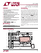


LTC1646
6
1646fa
PWRGD (Pin 4) :Open Drain Power Good Digital Output.
Connect the CPCI HEALTHY# signal to the PWRGD pin.
PWRGD remains low while V
3VOUT
≥ 2.9V and V
5VOUT
≥
4.65V. When either of the supplies falls below its power
good threshold voltage, PWRGD will go high after a 50µs
deglitching time.
5V
OUT
(Pin 5): 5V Output Sense. The PWRGD pin will not
pull low until the 5V
OUT
pin voltage exceeds 4.65V. If no 5V
input supply is available, tie the 5V
OUT
pin to the 3V
OUT
pin
in order to disable the 5V
OUT
power good function.
GND (Pin 6): Chip Ground
3V
OUT
(Pin 7): 3.3V Output Sense. The PWRGD pin will not
pull low until the 3V
OUT
pin voltage exceeds 2.90V. If no
3.3V input supply is available, tie the 3V
OUT
pin to the
5V
OUT
pin.
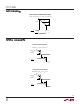
3V
IN
(Pin 8): 3.3V Supply Sense Input. An undervoltage
lockout circuit prevents the switches from turning on
when the voltage at the 3V
IN
pin is less than 2.5V. If no 3.3V
input supply is available, connect a diode between 5V
IN
and 3V
IN
(tie anode to 5V
IN
and cathode to 3V
IN
). See
Figure 11.
RESETOUT (Pin 1): Open Drain Digital Output. Connect
the CPCI LOCAL_PCI_RST# signal to the RESETOUT pin.
RESETOUT is the logical combination of RESETIN and
PWRGD (see Table 4).
TIMER (Pin 2): Current Fault Inhibit Timing Input. Connect
a capacitor from TIMER to GND. With the chip turned off,
the TIMER pin is internally held at GND. When the chip is
turned on, a 5µA pull-up current source is connected to
TIMER. Current limit and voltage compliance faults will be
ignored until the voltage at the TIMER pin is greater than
1.25V.
FAULT (Pin 3): Open Drain Digital I/O. FAULT is pulled low
when a current limit fault is detected. Faults are ignored
while the voltage at the TIMER pin is less than 1.25V. Once
the TIMER cycle is complete, FAULT will pull low and the
chip will latch off in the event of an overcurrent fault. The
chip will remain latched in the off state until the OFF/ON pin
is cycled high then low or the power is cycled.
Forcing the FAULT pin low with an external pull-down will
cause the chip to be latched into the off state after a 21µs
deglitching time.
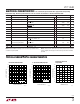
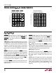
TYPICAL PERFOR A CE CHARACTERISTICS
UW
RESETOUT, PWRGD and FAULT
Output Low Voltage vs I
SINK
5V
OUT
/3V
OUT
Discharge
Impedance vs Temperature
–50 –25 0 25 50 75 100
TEMPERATURE (°C)
3V
OUT
/5V
OUT
DISCHARGE IMPEDANCE (Ω)
1646 G23
180
160
140
120
100
80
60
40
20
0
012 3 4 5
I
SINK
(mA)
OUTPUT LOW VOLTAGE (V)
1646 G22
1.0
0.9
0.8
0.7
0.6
0.5
0.4
0.3
0.2
0.1
0
90°C
25°C
–45°C
UU
U
PI FU CTIO S