
Datasheet

5
LTC1686/LTC1687
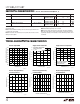
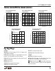
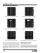
TYPICAL PERFORMANCE CHARACTERISTICS
UW
Receiver Propagation Delay
vs Temperature
TEMPERATURE (°C)
–50 –25
0
PROPAGATION DELAY (ns)
10
25
0
50
75
1686/87 G09
5
20
15
25
100
125
Driver Propagation Delay
vs Temperature
TEMPERATURE (°C)
–20
0
PROPAGATION DELAY (ns)
5
10
15
20
25
0
20 40 60
1686/87 G07
80 100
Receiver Maximum Data Rate
vs Input Overdrive
RECEIVER INPUT DIFFERENTIAL (V)
0.3
40
50
70
0.6 1.0
1686/87 G10
30
20
0.4 0.5
0.7 1.5 2.5
10
0
60
DATA RATE (Mbps)
T
A
= 25°C
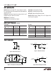
Driver Propagation Delay
vs Driver Input Voltage
DRIVER INPUT VOLTAGE (V)
2.5
PROPAGATION DELAY (ns)
15
20
25
4.5
1686/87 G08
10
5
0
3.0
3.5
4.0
5.0
t
LH
V
DD
= 5V
INPUT THRESHOLD = 1.5V
T
A
= 25°C
t
HL
Driver Propagation Delay
vs Capacitive Load
LOAD CAPACITANCE (pF)
5
16.0
PROPAGATION DELAY (ns)
16.5
17.0
17.5
18.0
19.0
15
25 50 75
1686/87 G11
100 150
18.5
T
A
= 25°C
PIN FUNCTIONS
UUU
LTC1686
V
DD
(Pin 1): Positive Supply, 5V to ±5%. Bypass with
0.1µF ceramic capacitor.
R (Pin 2): Receiver Output. If A ≥ B by 300mV, then R will
be high. If A ≤ B by 300mV, then R will be low.
D (Pin 3): Driver Input. Controls the states of the Y and Z
outputs. Do not float.
GND
(Pin 4): Ground.
Y (Pin 5): Noninverting Driver Output.
Z (Pin 6): Inverting Driver Output.
B (Pin 7): Inverting Receiver Input.
A (Pin 8): Noninverting Receiver Input.
LTC1687
NC (Pins 1, 8, 13): No Connection.
R (Pin 2): Receiver Output. If A ≥ B by 300mV, then R will
be high. If A ≤ B by 300mV, then R will be low.
RE (Pin 3): Receiver Enable. RE = low enables the receiver.
RE = high forces receiver output into high impedance
state. Do not float.