
Datasheet

8
LTC1686/LTC1687
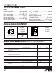
EQUIVALE T I PUT NETWORKS
U
U
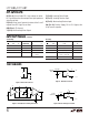
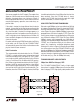
Figure 9. Input Thevenin Equivalent
A
B
1686/87 F09
≥22k
3.3V
≥22k
3.3V
RE = 0 OR 1, V
DD
= 5V V
DD
= 0V
A
B
≥22k
≥22k
APPLICATIONS INFORMATION
WUU
U
THEORY OF OPERATION
Unlike typical CMOS transceivers whose propagation
delay can vary by as much as 500% from package to
package and show significant temperature drift, the
LTC1686/LTC1687 employ a novel architecture that pro-
duces a tightly controlled and temperature compensated
propagation delay. The differential timing skew is also
minimized between rising and falling output edges of the
receiver output and the complementary driver outputs.
The precision timing features of the LTC1686/LTC1687
reduce overall system timing constraints by providing a
narrow ±3.5ns window during which valid data appears at
the receiver/driver output. The driver and receiver will
have propagation delays that typically match to within 1ns.
In clocked data systems, the low skew minimizes duty
cycle distortion of the clock signal. The LTC1686/LTC1687
can be used at data rates of 52Mbps with less than 5% duty
cycle distortion (depending on cable length). When a clock
signal is used to retime parallel data, the maximum recom-
mended data transmission rate is 26Mbps to avoid timing
errors due to clock distortion.
FAIL-SAFE FEATURES
The LTC1686/LTC1687 have a fail-safe feature that guar-
antees the receiver output to be in a logic HIGH state when
the inputs are either shorted or left open (note that when
inputs are left open, large external leakage currents might
override the fail-safe circuitry). In order to maintain good
high frequency performance, it is necessary to slow down
the transient response of the fail-safe feature. When a line
fault is detected, the output will go HIGH typically in 2µs.
Note that the LTC1686/LTC1687 guarantee receiver fail-
safe performance over the
entire
(–7V to 12V) common
mode range!
When the inputs are accidentally shorted (by cutting
through a cable, for example), the short circuit fail-safe
feature will guarantee a high output logic level. Note also
that if the line driver is removed and the ground terminated
resistors are left in place, the receiver will see this as a
“short” and output a logic HIGH. Both of these fail-safe
features will keep the receiver from outputting false data
pulses under line fault conditions.
Thermal shutdown and short-circuit protection prevent
latchup damage to the LTC1686/LTC1687 during fault
conditions.
OUTPUT SHORT-CIRCUIT PROTECTION
The LTC1686/LTC1687 employ voltage sensing short-
circuit protection at the output terminals of both the driver
and receiver. For a given input polarity, this circuitry
determines what the correct output level should be. If the
output level is different from the expected, it shuts off the
big output devices. For example, if the driver input is >2V,
it expects the “A” output to be >3.25V and the “B” output
to be <1.75V. If the “A” output is subsequently shorted to
a voltage below V
DD
/2, this circuitry shuts off the big
output devices and turns on a smaller device in its place