
Datasheet

2
LTC1686/LTC1687
A
U
G
W
A
W
U
W
ARB
S
O
LU
T
EXI T
I
S
(Note 1)
Supply Voltage (V
DD
) .............................................. 10V
Control Input Currents .................... –100mA to 100mA
Control Input Voltages .................. –0.5V to V
DD
+ 0.5V
Driver Input Voltages .................... –0.5V to V
DD
+ 0.5V
Driver Output Voltages ................................. +12V/–7V
Receiver Input Voltages ................................ +12V/–7V
Receiver Output Voltages ............. –0.5V to V
DD
+ 0.5V
Receiver Input Differential ...................................... 10V
Driver Short-Circuit Duration
(V
OUT
: –7V to 10V) ..................................... Indefinite
Receiver Short-Circuit Duration
(V
OUT
: 0V to V
DD
) ........................................ Indefinite
Operating Temperature Range
LTC1686C/LTC1687C ............................. 0°C to 70°C
LTC1686I/LTC1687I .......................... – 40°C to 85°C
Storage Temperature Range ................ – 65°C to 150°C
Lead Temperature (Soldering, 10 sec)................. 300°C
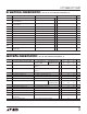
SYMBOL PARAMETER CONDITIONS MIN TYP MAX UNITS
V
OD1
Differential Driver Output (Unloaded) I
OUT
= 0 ● V
DD
V
V
OD2
Differential Driver Output (With Load) R = 50Ω (RS422) 2.0 V
R = 27Ω (RS485), Figure 1
● 1.5 V
DD
V
∆V
OD
Change in Magnitude of Driver Differential R = 27Ω or 50Ω, Figure 1 ● 0.2 V
Output Voltage for Complementary
Output States
V
OC
Driver Common Mode Output Voltage R = 27Ω or 50Ω, V
DD
= 5V, Figure 1 ● 23V
∆V
OC
Change in Magnitude of Driver Common R = 27Ω or 50Ω, Figure 1 ● 0.2 V
Mode Output Voltage for Complementary
Output States
V
IH
Input High Voltage D, DE, RE ● 2V
V
IL
Input Low Voltage D, DE, RE ● 0.8 V
I
IN1
Input Current D, DE, RE ● –1 1 µA
I
IN2
Input Current (A, B) V
A
, V
B
= 12V, V
DD
= 0V or 5.25V ● 500 µA
V
A
, V
B
= – 7V, V
DD
= 0V or 5.25V ● –500 µA
V
TH
Differential Input Threshold Voltage –7V ≤ V
CM
≤ 12V ● – 0.3 0.3 V
for Receiver
∆V
TH
Receiver Input Hysteresis V
CM
= 0V 25 mV
V
OH
Receiver Output High Voltage I
OUT
= – 4mA, V
ID
= 300mV ● 3.5 4.8 V
Consult factory for Industrial and Military grade parts.
V
DD
= 5V ± 5% unless otherwise noted (Notes 2, 3).
DC ELECTRICAL CHARACTERISTICS
T
JMAX
= 125°C, θ
JA
= 150°C/W
WU
U
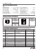
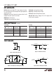
PACKAGE
/
O
RDER I FOR ATIO
LTC1687CS
LTC1687IS
T
JMAX
= 125°C, θ
JA
= 90°C/ W
ORDER PART
NUMBER
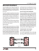
14
13
12
11
10
9
87
6
5
4
3
2
1
TOP VIEW
S PACKAGE
14-LEAD PLASTIC SO
NC
Y
NC
Z
B
NC
V
DD
D
GND
GND
R
RE
DE
A
R
D
ORDER PART
NUMBER
LTC1686CS8
LTC1686IS8
S8 PART MARKING
S8 PACKAGE
8-LEAD PLASTIC SO
1
2
3
4
8
7
6
5
TOP VIEW
V
DD
R
D
GND
A
B
Z
Y
R
D
1686
1686I