
Datasheet

5
LTC1688/LTC1689
16889fa
PIN FUNCTIONS
UUU
DI1 (Pin 1): Driver 1 Input. Do not float.
DO1A (Pin 2): Driver 1 Noninverting Output.
DO1B (Pin 3): Driver 1 Inverting Output.
EN (Pin 4, LTC1688): High True Enable Pin, enables all
four drivers. A low on Pin 4 and a high on Pin 12 will put
all driver outputs into a high impedance state. See
Function Tables for details. Do not float.
EN12 (Pin 4, LTC1689): Enables Drivers 1 and 2. A low on
Pin 4 will put the outputs of drivers 1 and 2 into a high
impedance state. See Function Tables for details. Do not
float.
DO2B (Pin 5): Driver 2 Inverting Output.
DO2A (Pin 6): Driver 2 Noninverting Output.
DI2 (Pin 7): Driver 2 Input. Do not float.
GND (Pin 8): Ground Connection. A good ground plane is
recommended for all applications.
DI3 (Pin 9): Driver 3 Input. Do not float.
DO3A (Pin 10): Driver 3 Noninverting Output.
DO3B (Pin 11): Driver 3 Inverting Output.
ENB (Pin 12, LTC1688): Low True Enable Pin, enables all
four drivers. A low on Pin 4 and a high on Pin 12 will put
all driver outputs into a high impedance state. See
Function Tables for details. Do not float.
EN34 (Pin 12, LTC1689): Enables Drivers 3 and 4. A low
on Pin 12 will put the outputs of drivers 3 and 4 into a high
impedance state. See Function Tables for details. Do not
float.
DO4B (Pin 13): Driver 4 Inverting Output.
DO4A (Pin 14): Driver 4 Noninverting Output.
DI4 (Pin 15): Driver 4 Input. Do not float.
V
DD
(Pin 16): Power Supply Input. This pin should be
bypassed with a 0.1µF ceramic capacitor as close to the
pin as possible. Recommended: V
DD
= 3V to 5.25V.
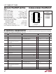
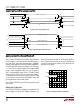
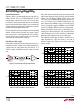
FU CTIO TABLES
U
U
LTC1688
INPUTS OUTPUTS
DI EN ENB OUTA OUTB
HH X H L
LH X L H
HX L H L
LX L L H
X L H HI-Z HI-Z
LTC1689
INPUTS OUTPUTS
DI EN12/EN34 OUTA OUTB
HHHL
LHLH
X L HI-Z HI-Z
1688/89 TC03
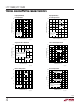
OUTPUT
UNDER TEST
C
L
S1
500
DD
V
Ω
S2
1688/89 TC01
A
B
R
R
OD
V
OC
V
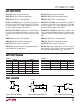
Figure 1. Driver DC Test Load
Figure 3. Driver Timing Test Load
DRIVER
1688/89 TC02
ENB (EN34)
DI
A
B
EN (EN12)
R
DIFF
C
L1
C
L2
Figure 2. Driver Timing Test Circuit
TEST CIRCUITS