
Datasheet

3
LTC1690
The ● denotes the specifications which apply over the full operating
temperature range, otherwise specifications are at T
A
= 25°C. V
CC
= 5V ±5% (Notes 2, 3)
DC ELECTRICAL CHARACTERISTICS
SYMBOL PARAMETER CONDITIONS MIN TYP MAX UNITS
V
OH
Receiver Output High Voltage I
O
= –4mA, V
ID
= 200mV ● 3.5 V
V
OL
Receiver Output Low Voltage I
O
= 4mA, V
ID
= –200mV ● 0.4 V
R
IN
Receiver Input Resistance –7V ≤ V
CM
≤ 12V ● 12 22 kΩ
I
CC
Supply Current No Load ● 260 600 µA
I
OSD1
Driver Short-Circuit Current, V
OUT
= HIGH –7V ≤ V
O
≤ 10V 35 250 mA
I
OSD2
Driver Short-Circuit Current, V
OUT
= LOW –7V ≤ V
O
≤ 10V 35 250 mA
I
OZ
Driver Three-State Current (Y, Z) –7V ≤ V
O
≤ 10V, V
CC
= 0V ● 5 200 µA
I
OSR
Receiver Short-Circuit Current 0V ≤ V
O
≤ V
CC
● 785mA
t
PLH
Driver Input to Output, Figure 3, Figure 4 R
DIFF
= 54Ω, C
L1
= C
L2
= 100pF ● 10 22.5 60 ns
t
PHL
Driver Input to Output, Figure 3, Figure 4 R
DIFF
= 54Ω, C
L1
= C
L2
= 100pF ● 10 25 60 ns
t
SKEW
Driver Output to Output, Figure 3, Figure 4 R
DIFF
= 54Ω, C
L1
= C
L2
= 100pF ● 2.5 15 ns
t
r
, t
f
Driver Rise or Fall Time, Figure 3, Figure 4 R
DIFF
= 54Ω, C
L1
= C
L2
= 100pF ● 21340 ns
t
PLH
Receiver Input to Output, Figure 3, Figure 5 R
DIFF
= 54Ω, C
L1
= C
L2
= 100pF ● 30 94 160 ns
t
PHL
Receiver Input to Output, Figure 3, Figure 5 R
DIFF
= 54Ω, C
L1
= C
L2
= 100pF ● 30 89 160 ns
t
SKD
|t
PLH
– t
PHL
|, Differential Receiver Skew, Figure 3, Figure 5 R
DIFF
= 54Ω, C
L1
= C
L2
= 100pF 5 ns
f
MAX
Maximum Data Rate, Figure 3, Figure 5 R
DIFF
= 54Ω, C
L1
= C
L2
= 100pF ● 5 Mbps
Note 1: Absolute Maximum Ratings are those values beyond which the life
of the device may be impaired.
Note 2: All currents into device pins are positive; all currents out of device
pins are negative. All voltages are referenced to device ground unless
otherwise specified.
Note 3: All typicals are given for V
CC
= 5V and T
A
= 25°C.
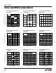
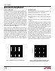
TYPICAL PERFOR A CE CHARACTERISTICS
UW
TEMPERATURE (°C)
–55 –35 –15 5 25 45 65 85 105 125
RECEIVER INPUT THRESHOLD VOLTAGE (mV)
1690 G01
0
–20
–40
–60
–80
–100
–120
–140
–160
–180
–200
V
CC
= 5V
V
CM
= 12V
V
CM
= 0V
V
CM
= –7V
TEMPERATURE (°C)
–55 –35 –15 5 25 45 65 85 105 125
RECEIVER INPUT THRESHOLD VOLTAGE (mV)
1690 G02
0
–20
–40
–60
–80
–100
–120
–140
–160
–180
–200
V
CC
= 5V
V
CM
= 12V
V
CM
= –7V
V
CM
= 0V
TEMPERATURE (°C)
–55 –35 –15 5 25 45 65 85 105 125
RECEIVER HYSTERESIS (mV)
1690 G03
100
90
80
70
60
50
40
30
20
10
0
V
CC
= 5V
V
CM
= 12V
V
CM
= –7V
V
CM
= 0V
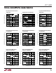
Receiver Input Threshold Voltage
(Output High) vs Temperature
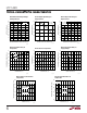
Receiver Input Threshold Voltage
(Output Low) vs Temperature
Receiver Hysteresis vs
Temperature