
Datasheet

7
LTC1690
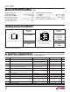
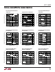
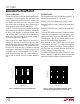
SWITCHI G TI E WAVEFOR S
UWW
–V
O
D
3V
0V
t
PLH
V
O
= V(A) – V(B)
V
O
Z
Y
t
SKEW
t
SKEW
t
r
f = 1MHz, t
r
≤ 10ns, t
f
≤ 10ns
1.5V
90%
10%
50%
t
PHL
t
f
1.5V
90%
10%
50%
V
O
1/2 V
O
1690 F04
Figure 4. Driver Propagation Delays
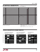
f = 1MHz, t
r
≤ 10ns, t
f
≤ 10ns
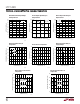
NOTE: t
SKD
= |t
PHL
– t
PLH
|
INPUT
OUTPUT
A – B
R
V
OD2
–V
OD2
5V
V
OL
t
PHL
0V
1.5V
t
PLH
0V
1.5V
1690 F05
Figure 5. Receiver Propagation Delays
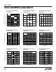
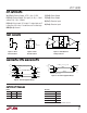
FUNCTION TABLES
UU
Driver
DZY
101
010
Receiver
A – B R
≥ –0.01V 1
≤ –0.20V 0
Inputs Open 1
Inputs Shorted 1
Note: Table valid with or without termination resistors.
1690 F01
Y
Z
R
R
V
OD2
V
OC
1690 F02
Y
Z
60Ω
375Ω
V
OD3
V
TST
–7V TO 12V
375Ω
1690 F03
D
Y
Z
R
DIFF
A
B
15pF
C
L1
C
L2
R
+
+
+
Figure 1. Driver
DC Test Load #1
Figure 2. Driver
DC Test Load #2
Figure 3. Driver/Receiver
Timing Test Load
TEST CIRCUITS
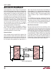
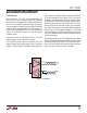
PIN FUNCTIONS
UUU
V
CC
(Pin 1): Positive Supply. 4.75V < V
CC
< 5.25V.
R (Pin 2): Receiver Output. R is high if (A – B) ≥ –10mV
and low if (A – B) ≤ –200mV.
D (Pin 3): Driver Input. If D is high, Y is taken high and Z
is taken low. If D is low, Y is taken low and Z is taken high.
GND (Pin 4): Ground.
Y (Pin 5): Driver Output.
Z (Pin 6): Driver Output.
B (Pin 7): Receiver Input.
A (Pin 8): Receiver Input.