
Datasheet


5
LTC1694-1
16941fa
APPLICATIONS INFORMATION
WUU
U
SMBus Overview
SMBus communication protocol employs open-drain
drives with resistive or current source pull-ups. This pro-
tocol allows multiple devices to drive and monitor the bus
without bus contention. The simplicity of resistive or fixed
current source pull-ups is offset by the slow rise times
resulting when bus capacitance is high. Rise times can be
improved by using lower pull-up resistor values or higher
fixed current source values, but the additional current
increases the low state bus voltage, decreasing noise
margins. Slow rise times can seriously impact data reli-
ability, enforcing a maximum practical bus speed well
below the established SMBus maximum transmission rate.
Theory of Operation
The LTC1694-1 overcomes these limitations by providing
a 2.2mA pull-up current only during positive bus transi-
tions to quickly slew any bus capacitance. Therefore, rise
time is dramatically improved, especially with maximum
SMBus loading conditions.
The LTC1694-1 has separate but identical circuitry for
each SMBus output pin. The circuitry consists of a positive
edge slew rate detector and a voltage comparator.
The 2.2mA pull-up current is only turned on if the voltage
on the SMBus line voltage is greater than the 0.65V
comparator threshold voltage and the positive slew rate of
the SMBus line is greater than the 0.2V/µs threshold of the
slew rate detector. The pull-up current remains on until the
voltage on the SMBus line is within 0.5V of V
CC
and/or the
slew rate drops below 0.2V/µs.
Selecting the Values of R
S
and R
P
An external pull-up resistor R
P
is required in each SMBus
line to supply a steady state pull-up current if the SMBus
is at logic zero. This pull-up current is used for slewing the
SMBus line during the initial portion of the positive transi-
tion in order to activate the LTC1694-1 2.2mA pull-up
current.
Using an external R
P
to supply the steady state pull-up
current permits the user the freedom to adjust rise time
versus fall time as well as defining the low state logic level
(V
OL
).
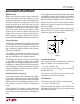
For I/O stage protection from ESD and high voltage spikes
on the SMBus, a series resistor R
S
(Figure 2) is sometimes
added to the open-drain driver of the bus agents. This is
especially common in SMBus-controlled smart batteries.
Both the values of R
P
and R
S
must be chosen carefully to
meet the low state noise margin and all timing require-
ments of the SMBus.
A discussion of the electrical parameters affected by the
values of R
S
and R
P
, as well as a general procedure for
selecting the values of R
S
and R
P
follows.
Figure 2
V
CC
R
S
C
BUS
SMBus
R
ON
1694-1 F02
DATA
IN
DATA
OUT
R
P
Low State Noise Margin
A low value of V
OL
, the low state logic level, is desired for
good noise margin. V
OL
is calculated as follows:
V
OL
= (R
L
• V
CC
)/(R
L
+ R
P
) (1)
R
L
is the series sum of R
S
and R
ON
, the on-resistance of
the open-drain driver.
Increasing the value of R
P
decreases the value of V
OL
.
Increasing R
L
increases the value of V
OL
.
Initial Slew Rate
The initial slew rate, SR, of the Bus is determined by:
SR = (V
CC
– V
OL
)/(R
P
• C
BUS
) (2)
SR must be greater than SR
THRES
, the LTC1694-1 slew
rate detector threshold (0.5/µs max) in order to activate
the 2.2mA pull-up current.