
Datasheet


6
LTC1694-1
16941fa
APPLICATIONS INFORMATION
WUU
U
SMBus Rise Time
Rise time of an SMBus line is derived using equations 3,
4 and 5.
t
r
= t
1
+ t
2
(3)
t
1
= –R
P
• C
BUS
• ln[(V
THRES
– V
CC
)/
(V
ILMAX
– 0.15 – V
CC
)] (4)
if (V
ILMAX
– 0.15) > V
THRES
, then t
1
= 0µs.
t
2
= –R
P
• C
BUS
• ln{[V
IHMIN
+ 0.15 – V
CC
–
(R
P
• I
PULL-UP
)]/[V
THRES
– V
CC
– (R
P
• I
PULL-UP
)]} (5)
By ignoring the current through R
P
, a simplified version
of equation 3 is obtained:
t
2
= (V
IHMIN
+ 0.15 – V
THRES
) • C
BUS
/I
PULL-UP
(6)
For an SMBus system, V
ILMAX
= 0.8V and V
IHMIN
= 2.1V.
For the LTC1694-1, typically V
THRES
= 0.65V and I
PULL-UP
= 2.2mA.
C
BUS
is the total capacitance of the SMBus line.
Increasing the value of R
P
increases the rise time.
SMBus Fall Time
Fall time of an SMBus line is derived using equation 7:
t
f
= R
T
• C
BUS
• ln{[0.9 • (R
P
+ R
L
) – R
L
]/
[(V
ILMAX
– 0.15) • (R
P
+ R
L
)/V
CC
– R
L
]} (7)
where R
T
is the parallel equivalent of R
P
and R
L
.
The rise and fall time calculation for an I
2
C system is as
follows.
I
2
C Bus Rise and Fall Time
Rise time of an I
2
C line is derived using equation 8.
t
r
= –R
P
• C
BUS
• ln{[V
IHMIN
– V
CC
– (R
P
• I
PULL-UP
)]/
[V
ILMAX
– V
CC
– (R
P
• I
PULL-UP
)]} (8)
Fall time of an I
2
C line is derived using equation 9:
t
f
= R
T
• C
BUS
• ln{[(V
IHMIN
/V
CC
) • (R
P
+ R
L
) – R
L
]/
[(V
ILMAX
/V
CC
) • (R
P
+ R
L
) – R
L
]} (9)
For an I
2
C system with fixed input levels, V
ILMAX
= 1.5V
and V
IHMIN
= 3V.
For an I
2
C system with V
CC
related input levels, V
ILMAX
=
0.3V
CC
and V
IHMIN
= 0.7V
CC
.
C
BUS
is the total capacitance of the I
2
C line.
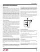
A general procedure for selecting R
P
and R
L
is as follows:
1. R
L
is first selected based on the I/O protection require-
ment. Generally, an R
S
of 100Ω is sufficient for high
voltage spike and ESD protection. R
ON
is determined by
the size of the open-drain driver, a large driver will have
a lower R
ON
.
2. Next, the value of R
P
is determined based on the rise and
fall time requirements using equations 3 to 7 (for an
SMBus system) or 8 and 9 (for an I
2
C system). The
value chosen for R
P
must ensure that both the rise and
fall time specifications are met simultaneously.
3. After R
P
and R
L
are selected, use equations 1 and 2 to
check if the V
OL
and SR requirements are fulfilled.
If SR is too low, decrease the value of R
P
. If V
OL
is too high,
increase the value of R
P
.
SMBus Design Example
Given the following conditions and requirements:
V
CC
= 3.3V nom
V
OL
= 0.4V max
C
BUS
= 200pF max
V
ILMAX
= 0.8V, V
IHMIN
= 2.1V
t
r
= 0.8µs max, t
f
= 0.3µs max
If an R
S
of 500Ω is used and the max R
ON
of the driver
is 200Ω, then R
L
= 500 + 200 = 700Ω. Using the max
V
THRES
of 0.9V and a min I
PULL-UP
of 1mA.
Using equation 6 to calculate the approximate value of t
2
:
t
2
= (2.1 + 0.15 – 0.9) • [(200 • 10
–12
)/(1 • 10
–3
)]
= 0.27µs
t
1
= 0.8 – 0.27 = 0.53µs
Using equation 4 to find the required R
P
to meet t
r
:
R
P
= –t
1
/{C
BUS
• ln[(V
THRES
– V
CC
)/
(V
ILMAX
– 0.15 – V
CC
)]} = 27k
R
T
= (R
P
• R
L
)/(R
P
+ R
L
)