
Datasheet


LTC1726
9
1726fd
For more information www.linear.com/LTC1726
applicaTions inForMaTion
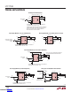
Figure 3 contains a simple circuit for 5V systems that can’t
risk the RST output going high in the 3.1V to 4.15V range
(possibly due to very slow rise time on the 5V supply).
Diode D1 powers the LTC1726-5 while dropping ≈0.6V
from the V
CC5
pin to the V
CC3
pin. This prevents the part’s
internal override circuit from being activated. Without the
override circuit active, the RST pin stays low until V
CC5
reaches V
RT5
≅ 4.675V. (See Figure 4.)
Figure 4. RST Output Voltage
Characteristics of the Circuit in Figure 3
Figure 3. LTC1726-5 Monitoring a Single 5V
Supply. D1 Used to Avoid RST High Near 3.1V
to 4V (See Figure 2).
Watchdog Timer
The watchdog circuit monitors a µP’s activity. The µP is
required to change the logic state of the WDI pin on a
periodic basis in order to clear the watchdog timer and
prevent the LTC1726 from issuing a reset.
During power-up, the watchdog timer remains cleared
while reset is asserted. As soon as the reset timer times
out, the watchdog timer is started. The watchdog timer
will continue to run until a transition is detected on the
WDI input
or until the watchdog timer times out. Once the
watchdog timer times out, the internal circuitry asserts
the reset and starts the reset timer. When the reset timer
times out and reset is deasserted, the watchdog timer is
again started. If no WDI transition is received within the
watchdog time-out period, the reset will be reasserted at
the end of the watchdog time-out period. If a transition is
received on the WDI input during the watchdog time-out
period, the watchdog timer will be restarted and reset will
remain deasserted.
Selecting the Reset and Watchdog
Time-Out Capacitors
The reset time-out period is adjustable in order to accom-
modate a variety of µP applications. The reset time-out
period, t
RT
, is adjusted by connecting a capacitor, C
RT
,
between the RT pin and ground. The value of this capacitor
is determined as follows:
C
RT
= t
RT
/3.30
with C
RT
in pF and t
RT
in µs (i.e., 1500pF ⇒ 4.95ms).
The capacitor should be a low leakage type. A ceramic
capacitor is recommended.
The watchdog period is also adjustable so that the watchdog
time-out period can be optimized for software execution.
The watchdog time-out
period, t
WT
, is adjusted by connect-
ing a capacitor, C
WT
, between the WT pin and ground. Once
the optimum watchdog time-out period (t
WT
) is determined,
the value of the capacitor is calculated as follows:
C
WT
= t
WT
/21.8
with C
WT
in pF and t
WT
in µs (i.e., 1500pF ⇒ 32.7ms).
The capacitor should be a low leakage type. A ceramic
capacitor is recommended.
V
CC3
V
CC5
V
CCA
GND
6
1
2
3
4
RST
LTC1726-5
1726 F03
TO SYSTEM
RESET
R1
10k
5V
0.1µF
D1
D1: MMBD914 OR EQUIVALENT
PINS 5, 7 AND 8 NOT SHOWN FOR CLARITY
V
CC5
(V)
0 0.5 1.0 1.5 2.0 2.5 3.0 3.5 4.0 4.5 5.0
RST OUTPUT VOLTAGE (V)
1726 F04
5
4
3
2
1
0
V
CC5
= V
CCA
= 0V TO 5V
10k PULL-UP FROM RST TO V
CC5
T
A
= 25°C
LTC1726-2.5 Override Functions
The V
CCA
pin, if unused, can be tied to either V
CC3
or
V
CC25
. This is an obvious solution since the trip points for
V
CC3
and V
CC25
will always be greater than the trip point
for V
CCA
. Likewise, the V
CC25
, if unused, can be tied to
V
CC3
. V
CC3
must always be used. Tying V
CC3
to V
CC25
and
operating off of a 2.5V supply will result in the continuous
assertion of RST.
Downloaded from Arrow.com.Downloaded from Arrow.com.Downloaded from Arrow.com.Downloaded from Arrow.com.Downloaded from Arrow.com.Downloaded from Arrow.com.Downloaded from Arrow.com.Downloaded from Arrow.com.Downloaded from Arrow.com.