
Datasheet


15
LTC1755/LTC1756
APPLICATIO S I FOR ATIO
WUUU
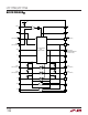
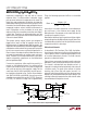
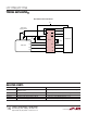
Figure 9. LTC1755/LTC1756 State Diagram
DEACTIVATION
NO
FAULT
FAULT
1755 F09
POWER OFF
IDLE
DEACTIVATION
ALARM
ACTIVE
FAULT
TIMEOUT
PWR = DV
CC
PWR = DV
CC
PWR = 0V
PRES ≠ NC/NO
FAULT > 5µs
or
PRES ≠ NC/NO
The only possible next state is Idle/Deactivation which is
achieved by disabling the LTC1755/LTC1756 via the PWR
pin (i.e., PWR = DV
CC
).
The alarm indication can be cleared by rapidly cycling the
PWR pin. However, a new activation cycle will not begin
until V
CC
is or has dropped below approximately 1V.
ACTIVE
V
CC
= 3V or 5V (as determined by the 5V/3V pin)
RST = R
IN
, CLK = C
IN
I/O, AUX2, AUX1, DATA, AUX2IN, AUX1IN = Ready for
data (after READY becomes low)
CARD = PRES ⊕ NC/NO
ALARM = H
FAULT TIMEOUT
Same as Active except:
The duration of a fault is being measured. If the fault
duration exceeds 5µs then the Alarm/Deactivation state
follows. If the fault duration is less than 5µs, then the
device is returned to the Active state.
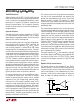
Dimensions in inches (millimeters) unless otherwise noted.
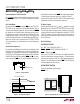
GN Package
16-Lead Plastic SSOP (Narrow 0.150)
(LTC DWG # 05-08-1641)
U
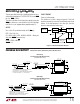
PACKAGE DESCRIPTIO
GN Package
24-Lead Plastic SSOP (Narrow 0.150)
(LTC DWG # 05-08-1641)
GN16 (SSOP) 1098
* DIMENSION DOES NOT INCLUDE MOLD FLASH. MOLD FLASH
SHALL NOT EXCEED 0.006" (0.152mm) PER SIDE
** DIMENSION DOES NOT INCLUDE INTERLEAD FLASH. INTERLEAD
FLASH SHALL NOT EXCEED 0.010" (0.254mm) PER SIDE
0.016 – 0.050
(0.406 – 1.270)
0.015
± 0.004
(0.38 ± 0.10)
× 45°
0° – 8° TYP
0.007 – 0.0098
(0.178 – 0.249)
0.053 – 0.068
(1.351 – 1.727)
0.008 – 0.012
(0.203 – 0.305)
0.004 – 0.0098
(0.102 – 0.249)
0.0250
(0.635)
BSC
12
3
4
5
6
7
8
0.229 – 0.244
(5.817 – 6.198)
0.150 – 0.157**
(3.810 – 3.988)
16
15
14
13
0.189 – 0.196*
(4.801 – 4.978)
12 11 10
9
0.009
(0.229)
REF
GN24 (SSOP) 1098
* DIMENSION DOES NOT INCLUDE MOLD FLASH. MOLD FLASH
SHALL NOT EXCEED 0.006" (0.152mm) PER SIDE
** DIMENSION DOES NOT INCLUDE INTERLEAD FLASH. INTERLEAD
FLASH SHALL NOT EXCEED 0.010" (0.254mm) PER SIDE
0.016 – 0.050
(0.406 – 1.270)
0.015
± 0.004
(0.38 ± 0.10)
× 45°
0° – 8° TYP
0.007 – 0.0098
(0.178 – 0.249)
0.053 – 0.068
(1.351 – 1.727)
0.008 – 0.012
(0.203 – 0.305)
0.004 – 0.0098
(0.102 – 0.249)
0.0250
(0.635)
BSC
0.337 – 0.344*
(8.560 – 8.738)
12
3
4
5
6
7
8 9 10 11 12
0.229 – 0.244
(5.817 – 6.198)
0.150 – 0.157**
(3.810 – 3.988)
161718192021222324
15
14
13
0.033
(0.838)
REF
Information furnished by Linear Technology Corporation is believed to be accurate and reliable.
However, no responsibility is assumed for its use. Linear Technology Corporation makes no represen-
tation that the interconnection of its circuits as described herein will not infringe on existing patent rights.