
Datasheet


11
LTC1755/LTC1756
10kV ESD Protection
All Smart Card pins (CLK, RST, I/O, AUX1, AUX2, V
CC
and
GND) can withstand over 10kV of human body model ESD
in situ. In order to ensure proper ESD protection, careful
board layout is required. The GND pin should be tied
directly to a ground plane. The V
CC
capacitor should be
located very close to the V
CC
pin and tied immediately to
the ground plane.
Capacitor Selection
The style and value of capacitors used with the LTC1755/
LTC1756 determine several parameters such as output
ripple voltage, charge pump strength, Smart Card switch
debounce time and V
CC
discharge rate.
Due to the switching nature of a capacitive charge pump,
low equivalent series resistance (ESR) capacitors are
recommended for the capacitors at V
IN
and V
CC
. When-
ever the flying capacitor is switched to the V
CC
charge
storage capacitor, considerable current flows. The prod-
uct of this high current and the ESR of the output capacitor
can generate substantial voltage spikes on the V
CC
output.
These spikes may cause problems with the Smart Card or
may interfere with the regulation loop of the LTC1755/
LTC1756. Therefore, ceramic or tantalum capacitors are
recommended rather than higher ESR aluminum capaci-
tors. Between ceramic and tantalum, ceramic capacitors
generally have the lowest ESR. Some manufacturers have
developed low ESR tantalum capacitors but they can be
expensive and may still have higher ESR than ceramic
types. Thus, while they cannot be avoided, ESR spikes will
typically be lowest when using ceramic capacitors.
For ceramic capacitors there are several different materi-
als available to choose from. The choice of ceramic
material is generally based on factors such as available
capacitance, case size, voltage rating, electrical perfor-
mance and cost. For example, capacitors made of Y5V
material have high packing density, which provides high
capacitance for a given case size. However, Y5V capaci-
tors tend to lose considerable capacitance over the –40°C
to 85°C temperature range. X7R ceramic capacitors are
more stable over temperature but don’t provide the high
packing density. Therefore, large capacitance values are
generally not available in X7R ceramic.
The value and style of the flying capacitor are important
not only for the charge pump but also because they
provide the large debounce time for the Smart Card
detection channel. A 0.68µF X7R capacitor is a good
choice for the flying capacitor because it provides fairly
constant capacitance over temperature and its value is not
prohibitively large.
The charge storage capacitor on the V
CC
pin determines
the ripple voltage magnitude and the discharge time of the
Smart Card voltage. To minimize ripple, generally, a large
value is needed. However, to meet the V
CC
discharge rate
specification, the value should not exceed 20µF. A 10µF
capacitor can be used but the ripple magnitude will be
higher leading to worse apparent DC load regulation.
Typically a 15µF to 18µF Y5V ceramic capacitor is the best
choice for the V
CC
charge storage capacitor. For best
performance, this capacitor should be connected as close
as possible to the V
CC
and GND pins. Note that most of the
electrostatic discharge (ESD) current on the Smart Card
pins is absorbed by this capacitor.
The bypass capacitor at V
IN
is also important. Large dips
on the input supply due to ESR may cause problems with
the internal circuitry of the LTC1755/LTC1756. A good
choice for the input bypass capacitor is a 10µF Y5V style
ceramic
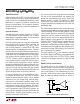
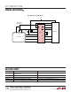
Dynamic Pull-Up Current Sources
The current sources on the bidirectional pins (DATA,
AUX2IN, AUX1IN, I/O, AUX2 and AUX1) are dynamically
activated to achieve a fast rise time with a relatively small
static current (Figure 1). Once a bidirectional pin is relin-
quished, a small start-up current begins to charge the
node. An edge rate detector determines if the pin is
Figure 1. Dynamic Pull-Up Current Sources
–
+
δV
δt
I
START
17556 F01
V
REF
BIDIRECTIONAL PIN
V
CC
OR DV
CC
APPLICATIO S I FOR ATIO
WUUU