
Datasheet


12
LTC1755/LTC1756
5V/µs, the following expression for R
PULL-UP
should be
applied:
R
VV
CpF
PULL UP
SUPPLY
PAR
−
=
()
()
–
–•
1
50 5 10
6
where C
PAR
is the extra capacitance on the bidirectional
pin and V
SUPPLY
is the minimum local supply for the
bidirectional pin. For example, on the smart card side, 3V
should be assumed for V
SUPPLY
.
Note that the addition of a pull-up resistor will give a higher
output voltage when the bidirectional pin pulls down. Care
should be taken so that the V
IL
or V
OL
specifications are not
compromised with this technique.
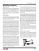
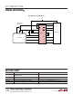
Bidirectional Channels
As described in Pin Functions (Pins 10/6), the bidirec-
tional channels allow transmission in only one direction at
a time. Figure 2 shows a simplified block diagram of one
of the three bidirectional channels. The three channels
operate in an identical fashion.
Figure 3 shows an example of normal transmit and receive
operations as well as the two possible collision scenarios.
If a channel is activated from one direction and an L is
imposed in the other direction before both sides return H
a collision results. The result of the collision is that the
receiving side (
Slave Side
) will remain low until it is
released, but the transmitting side (first side to go low or
Master Side
), will be allowed to return high if released. The
colliding L externally imposed on the slave side will not be
transmitted back through the channel.
released by comparing its slew rate with an internal
reference value. If a valid transition is detected, a large
pull-up current enhances the edge rate on the node. The
higher slew rate corroborates the decision to charge the
node thereby effecting a dynamic form of hysteresis. Once
the node has reached the power supply voltage the internal
comparator requires several hundred nanoseconds to
reset. Pulling down on the pin before the reset delay
expires will result in a momentary contention and a higher
current flow. Therefore, the comparator delay sets the
upper limit on the maximum data rate of the bidirectional
channels to about 500kHz.
The dynamic pull-up current sources are designed to
trigger with as much as 50pF of capacitive load on the
bidirectional pins. At approximately 90pF (or greater), the
edge rate on the node will be insufficient to trigger the edge
rate detector and the node will only ramp up at a rate given
by the I
START
current source and the load capacitance. In
these instances the edge rate of the bidirectional pin may
not meet the requirements of existing smart card stan-
dards. Therefore, it is recommended that the sum of both
explicit and parasitic capacitances on the bidirectional
pins be kept below 50pF.
If excessive capacitance (either explicit or parasitic) is
present on the bidirectional pins, the starting pull-up
current must also be increased. This can be accomplished
with a pull-up resistor to the respective supply. For the
smart card side (I/O, AUX1 and AUX2), the pull-up resis-
tor should be connected to V
CC
. For the microcontroller
side (DATA, AUX1IN and AUX2IN), the pull-up resistor
should be connected to DV
CC
on the LTC1755 (V
IN
on the
LTC1756). To maintain an edge rate of approximately
APPLICATIO S I FOR ATIO
WUUU
DV
CC
CS
DATA
CHARGE
PUMP
BIDIRECTIONAL
LATCH
I/O
TO
SMART CARD
TO
MICROCONTROLLER
V
CC
READY
3.5mA
17756 F02
Figure 2. Bidirectional Channel Simplified Block Diagram