
Datasheet


13
LTC1755/LTC1756
less than 10µA. If DV
CC
is 0V the current drops below 1µA.
When a Smart Card is present the LTC1755/LTC1756
operate with a quiescent current of only 60µA, thus the
majority of power is consumed by charge pump losses
and the card itself. If the card can be made to consume less
power during idle times a significant power savings will be
achieved. Whenever possible Clock Stop Mode should be
used (or alternatively a very low “idling” clock speed).
Furthermore, in the Active state, the bidirectional pins
should all be relinquished whenever possible since there
is some static current flow when a bidirectional pin is
pulled down.
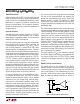
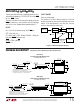
LTC1755
*
2N7002T1 (MOTOROLA)
TN2460T (TEMIC/SILICONIX)
I/O
R1
20k
TO
SMART CARD
17556 F04
*CONNECT GATE TO V
CC
FOR DV
CC
= 5V APPLICATIONS
CONNECT GATE TO DV
CC
OR DV
CC
LOGIC LEVEL SIGNAL
FOR DV
CC
≤ 3.3V APPLICATONS
5V
POWER
TO
MICROCONTROLLER
DATA
MN1
V
CC
DV
CC
Figure 4. I
2
C Level Translation Technique
I
2
C
TM
Compatibility
Some smart cards still require I
2
C compatibility. In the I
2
C
format it is permissible to impose an L before the signal
line has returned H. This is used, for example, as an
acknowledge signal. Such a scenario will cause a collision
as shown in Figure 3.
Figure 4 shows an analog level translation technique that
can be used along with the LTC1755 to support I
2
C smart
cards. In this technique it is important to connect the gate
of the external MOSFET to the lower of the two supplies
(i.e., the lower of V
CC
or DV
CC
). If DV
CC
is operating from
a fixed 5V supply, the gate of MN1 should be connected to
V
CC
. If DV
CC
is operating from a regulated 3.3V supply, the
gate of MN1 should be connected to DV
CC
. In the latter
case, the gate may need to be connected to a digital signal
ranging from 0V to DV
CC
so that it can be disabled when
the LTC1755 is in shutdown. Otherwise, the the LTC1755
will try to assert an L on the microcontroller side of the
channel when it is in shutdown.
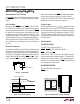
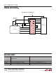
Supporting Synchronous and Asyncronous Cards
In synchronous/asynchronous applications it is neces-
sary to switch the CLK pin of the card socket from a free
running asynchronous clock to a controlled syncronous
clock. To avoid glitches and pulses shorter than the
minimum allowed pulse width, the circuit shown in Figure
5 should be used as a clock selection circuit. Note that for
this circuit to be effective the SYNC input should be held
constant while switching the ASYNC\SYNC control signal.
Low Power Operation
The LTC1755/LTC1756 are inherently low power devices.
When there is no Smart Card present the supply current is
Q
QD
TO C
IN
17556 F05
Q
ASYNC SYNC
ASYNC IN
SYNC IN
QD
Figure 5. Glitchless Clock Selection Circuit
APPLICATIO S I FOR ATIO
WUUU
I
2
C is a trademark of Philips Electronics N.V.
DATA
I/O
NORMAL
TRANSMIT
NORMAL
RECEIVE
I/O PULLED LOW DURING
TRANSMIT MODE (COLLISION)
DATA PULLED LOW DURING
RECEIVE MODE (COLLISION)
17556 F03
Figure 3. Possible Bidirectional Channel Scenarios