
Datasheet


6
LTC1755/LTC1756
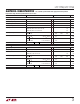
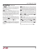
TYPICAL PERFOR A CE CHARACTERISTICS
UW
DV
CC
, V
IN
Supply Current
In Shutdown
DV
CC
INPUT VOLTAGE (V)
0
0
INPUT CURRENT (µA)
3.0
6.0
9.0
1.5
4.5
7.5
DV
CC
V
IN
1
234
17556 G10
56
V
IN
= 3V
T
A
= 25°C
V
IN
Shutdown Current
vs Input Voltage
INPUT VOLTAGE (V)
0
0
INPUT CURRENT (µA)
0.2
0.4
0.6
0.8
1.0
1
234
17556 G11
56
DV
CC
= 0
T
A
= 25°C
UU
U
PI FU CTIO S
PRES (Pin 1): (Input) Connects to the Smart Card acceptor’s
PRESENT indicator switch to detect if a card is inserted.
This pin has a pull-up current source so that a grounded
switch can be detected with no external components. The
pull-up current source is nonlinear, delivering higher
current when the PRES pin is above 1V but very little
current below 1V. This helps resist false card indications
due to leakage current. The activation state of the PRES pin
can be set by the NC/NO pin so that both normally open
(NO) and normally closed (NC) switches are easily recog-
nized (see NC/NO pin description).
DV
CC
sets the logic reference level for the PRES pin.
PWR (Pin 2): (Input) A low on the PWR pin places the
LTC1755/LTC1756 in the ACTIVE state enabling the charge
pump. The READY pin indicates when the card supply
voltage (V
CC
) has reached its final value and communica-
tion with the Smart Card is possible. The reset and clock
channels are enabled after READY goes low. The three I/
O channels are also enabled only after READY goes low,
however they may be disabled separately via the CS pin
(CS is not available on the LTC1756).
The falling edge of PWR latches the state of the 5V/3V pin.
After PWR is low, changes on the 5V/3V pin are ignored.
CS (Pin 3, LTC1755 Only): (Input) The CS pin enables the
three bidirectional I/O channels of the LTC1755. When the
I/O channels are disabled the Smart Card pins (I/O, AUX1,
AUX2) are forced to logic one and the controller pins
(DATA, AUX2IN, AUX1IN) are high impedance. CS can be
brought low along with PWR when the device is first
enabled, however communication with the Smart Card is
inhibited until V
CC
reaches its final value as indicated by a
low on the READY pin. CS does not affect the charge
pump, CLK or RST channels. On the LTC1756, CS is
internally connected to the PWR pin.
DV
CC
sets the logic reference level for the CS pin.
NC/NO (Pin 4, LTC1755 Only): (Input) This pin controls
the activation level of the PRES pin. When it is high (DV
CC
)
the PRES pin is active high. When it is low (GND) the PRES
pin is active low. In either case the presence of a Smart
Card is indicated by a low on the CARD output. When a
ground side normally open (NO) switch is used the NC/NO
pin should be grounded. When a ground side normally
closed (NC) switch is used the NC/NO pin should be
connected to DV
CC
. The LTC1756 is permanently config-
ured to accept a normally open switch.
LTC1755/LTC1756