
Datasheet
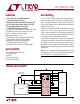


8
LTC1755/LTC1756
microseconds then the LTC1755/LTC1756 switch to the
Alarm state. This fault checking is only performed after the
V
CC
pin has reached its final value (as indicated by the
READY pin).
The clock channel is optimized for signal integrity in order
to meet the stringent duty cycle requirements of the EMV
specification. Therefore, to reduce power in low power
applications, clock stop mode is recommended when data
is not being exchanged.
CIN (Pins 13/9): (Input) Clock Input Pin from the Micro-
controller. During the Active state this signal appears on
the CLK pin after being level-shifted and buffered.
DV
CC
sets the logic reference level for the C
IN
pin.
RIN
(Pins 14/10): (Input) Reset Input Pin from the Micro-
controller. During the Active state this signal appears on
the RST pin after being level-shifted and buffered.
DV
CC
sets the logic reference level for the R
IN
pin.
DATA (Pins 15/11): (Input/Output) Microcontroller Side
Data I/O Pin. This pin is used for bidirectional data transfer
between the microcontroller and the Smart Card. The
microcontroller data pin must be open drain and must be
able to sink up to 250µA when driving the DATA pin low
due to the pull-up current source. The DATA pin becomes
high impedance during the Idle state or when CS is high
(see the State Diagram). It does not become active until the
READY signal goes low indicating that V
CC
is stable.
AUX2IN (Pin 16, LTC1755 Only): (Input/Output) Micro-
controller Side Auxiliary I/O pin. This pin is used for
bidirectional auxiliary data transfer between the micro-
controller and the Smart Card. It has the same character-
istics as the DATA pin.
AUX1IN (Pin 17, LTC1755 Only): (Input/Output) Micro-
controller Side Auxiliary I/O Pin. This pin is used for
bidirectional auxiliary data transfer between the micro-
controller and the Smart Card. It has the same character-
istics as the DATA pin.
C
+
, C
–
(Pins 18/12, 19/13): Charge Pump Flying Capaci-
tor Terminals. Optimum values for the flying capacitor
range from 0.68µF to 1µF. Best performance is achieved
with a low ESR X7R ceramic capacitor.
DV
CC
(Pin 20, LTC1755 Only): Supply Voltage for the
Microcontroller Side Digital Input and Input/Output Pins
(Typically 3V). If the charge pump input pin (V
IN
) is
powered from the same source as the microcontroller,
then DV
CC
should be connected directly to V
IN
. In this case
only one (10µF) input bypass capacitor is needed for the
LTC1755. If the DV
CC
pin is powered separately then it
should be bypassed separately with a 0.1µF capacitor. The
DV
CC
pin may be between 2V and 5.5V.
The DV
CC
pin is monitored for adequate voltage. If DV
CC
drops below approximately 1.5V the LTC1755 automati-
cally enters the Idle state. On the LTC1756, DV
CC
is
connected internally to V
IN
.
READY (Pins 21/14): (Output) Readiness Indicator of the
Smart Card Supply Voltage (V
CC
). When the LTC1755/
LTC1756 are placed in the Active state the soft-start
feature slowly ramps the V
CC
voltage. A low on the READY
pin indicates that V
CC
has reached its final value.
The READY pin also indicates if the LTC1756 is in Alarm
mode. The LTC1756 detects faults such as V
CC
underrange
for at least 5µs, overtemperature shutdown, CLK or RST
invalid output levels and card removal during Active
state. CLK or RST invalid and overtemperature faults are
detected only after V
CC
has reached its final value. V
CC
underrange and card removal during Active faults are
detected at any time during the Active period (i.e., once
PWR = 0V).
If the LTC1756 has been activated normally and V
CC
, the
card voltage, has reached its final value then READY will
go low indicating normal operation. If, following this, a
fault occurs and the LTC1756 enters the Alarm state, the
READY pin will return high.
In the event that a fault precedes the activation of V
CC
,
such as a direct short circuit from V
CC
to GND, the
LTC1756 will attempt to operate until the fault is detected
and then automatically shut down and enter the Alarm
state. In this case the READY pin will never go low after the
command to start the smart card is given (i.e., PWR = 0V).
If the LTC1755/LTC1756 enter the Alarm state they can
only be cleared by returning the PWR pin high.
UU
U
PI FU CTIO S
LTC1755/LTC1756