
Datasheet


LTC1799
10
1799fc
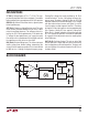
applicaTions inForMaTion
Once R
IN
/R
SET
is known, calculate R
SET
from:
R
SET
=
10MHz
N
•
10k
f
OSC(MAX)
•
V
IN(MAX)
− V
+
( )
+ V
RES
1+
R
IN
R
SET
V
RES
R
IN
R
SET
(3)
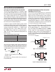
Maximum VCO Modulation Bandwidth
The maximum VCO modulation bandwidth is 10kHz; that
is, the LTC1799 will respond to changes in V
IN
at a rate
up to 25kHz. In lower frequency applications however, the
modulation frequency may need to be limited to a lower
rate to prevent an increase in output jitter. This lower limit
is the master oscillator frequency divided by 20, (f
OSC
/20).
In general, for minimum output jitter the modulation fre-
quency should be limited to f
OSC
/20 or 10kHz, whichever
is less. For best performance at all frequencies, the value
for f
OSC
should be the master oscillator frequency (N=1)
when V
IN
is at the lowest level.
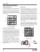
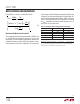
Table 2. Variation of V
RES
for Various Values of R
IN
|| R
SET
R
IN
|| R
SET
(V
IN
= V
+
) V
RES
, V
+
= 3V V
RES
, V
+
= 5V
10k 0.98V 1.06V
20k 1.03V 1.11V
40k 1.09V 1.17V
80k 1.13V 1.21V
160k 1.16V 1.24V
V
RES
= Voltage across R
SET
Note: All of the calculations above assume V
RES
= 1.1V, although V
RES
≈ 1.1V. For completeness,
Table 2 shows the variation of V
RES
against various parallel combinations of R
IN
and R
SET
(V
IN
= V
+
). Calulate first with V
RES
≈ 1.1V, then use Table 2 to get a better approximation of
V
RES
, then recalculate the resistor values using the new value for V
RES
.