
Datasheet


LTC1799
2
1799fc
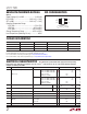
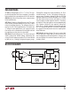
pin conFiguraTionabsoluTe MaxiMuM raTings
Supply Voltage (V
+
) to GND ......................... –0.3V to 6V
DIV to GND .....................................–0.3V to (V
+
+ 0.3V)
SET to GND .....................................–0.3V to (V
+
+ 0.3V)
Operating Temperature Range
LTC1799C ................................................ 0°C to 70°C
LTC1799I .............................................–40°C to 85°C
LTC1799H .......................................... –40°C to 125°C
Storage Temperature Range .................. –65°C to 150°C
Lead Temperature (Soldering, 10 sec) ...................300°C
(Note 1)
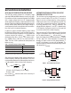
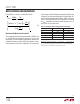
TOP VIEW
S5 PACKAGE
5-LEAD PLASTIC TSOT-23
1
2
3
V
+
GND
SET
5
4
OUT
DIV
T
JMAX
= 125°C, θ
JA
= 256°C/W
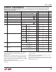
orDer inForMaTion
LEAD FREE FINISH TAPE AND REEL PART MARKING* PACKAGE DESCRIPTION TEMPERATURE RANGE
LTC1799CS5#PBF LTC1799CS5#TRPBF LTND 5-Lead Plastic TSOT-23 0°C to 70°C
LTC1799IS5#PBF LTC1799IS5#TRPBF LTNE 5-Lead Plastic TSOT-23 –40°C to 85°C
LTC1799HS5#PBF LTC1799HS5#TRPBF LTND 5-Lead Plastic TSOT-23 –40°C to 125°C
Consult LTC Marketing for parts specified with wider operating temperature ranges. *The temperature grade is identified by a label on the shipping container.
Consult LTC Marketing for information on non-standard lead based finish parts.
For more information on lead free part marking, go to: http://www.linear.com/leadfree/
For more information on tape and reel specifications, go to: http://www.linear.com/tapeandreel/
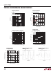
elecTrical characTerisTics
SYMBOL PARAMETER CONDITIONS MIN TYP MAX UNITS
∆f Frequency Accuracy
(Notes 2, 3)
V
+
= 5V 5kHz ≤ f ≤ 20MHz
5kHz ≤ f ≤ 20MHz, LTC1799C
5kHz ≤ f ≤ 20MHz, LTC1799I/H
1kHz ≤ f ≤ 5kHz
20MHz ≤ f ≤ 33MHz
l
l
±0.5
±2.5
±2.5
±1.5
±2
±2.5
%
%
%
%
%
V
+
= 3V 5kHz ≤ f ≤ 10MHz
5kHz ≤ f ≤ 10MHz, LTC1799C
5kHz ≤ f ≤ 10MHz, LTC1799I/H
1kHz ≤ f ≤ 5kHz
10MHz ≤ f ≤ 20MHz
l
l
±0.5
±2.5
±2.5
±1.5
±2
±2.5
%
%
%
%
%
R
SET
Frequency-Setting Resistor Range |∆f| < 1.5% V
+
= 5V
V
+
= 3V
5
10
200
200
kΩ
kΩ
f
MAX
Maximum Frequency |∆f| < 2.5%, Pin 4 = 0V V
+
= 5V
V
+
= 3V
33
20
MHz
MHz
f
MIN
Minimum Frequency |∆f| < 2.5%, Pin 4 = V
+
1 kHz
∆f/∆T Freq Drift Over Temp (Note 3) R
SET
= 31.6k
l
±0.004 %/°C
∆f/∆V Freq Drift Over Supply (Note 3) V
+
= 3V to 5V, R
SET
= 31.6k
l
0.05 0.1 %/V
Timing Jitter
(Note 4)
Pin 4 = V
+
Pin 4 = Open
Pin 4 = 0V
0.06
0.13
0.4
%
%
%
Long-Term Stability of Output Frequency 300 ppm/√kHr
The l denotes the specifications which apply over the full operating
temperature range, otherwise specifications are at T
A
= 25°C. V
+
= 2.7V to 5.5V, R
L
= 5k, C
L
= 5pF, unless otherwise noted. All
voltages are with respect to GND.