
Datasheet
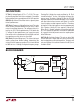


LTC1799
3
1799fc
elecTrical characTerisTics
Note 1: Stresses beyond those listed under Absolute Maximum Ratings
may cause permanent damage to the device. Exposure to any Absolute
Maximum Rating condition for extended periods may affect device
reliability and lifetime.
Note 2: Frequencies near 100kHz and 1MHz may be generated using two
different values of R
SET
(see the Table 1 in the Applications Information
section). For these frequencies, the error is specified under the following
assumption: 10k < R
SET
≤ 100k. The frequency accuracy for f
OSC
= 20MHz
is guaranteed by design and test correlation.
Note 3: Frequency accuracy is defined as the deviation from the
f
OSC
equation.
SYMBOL PARAMETER CONDITIONS MIN TYP MAX UNITS
Duty Cycle (Note 7) Pin 4 = V
+
or Open (DIV Either by 100 or 10)
Pin 4 = 0V (DIV by 1), R
SET
= 5k to 200k
l
l
49
45
50
50
51
55
%
%
V
+
Operating Supply Range
l
2.7 5.5 V
I
S
Power Supply Current R
SET
= 200k, Pin 4 = V
+
, R
L
= ∞ V
+
= 5V
l
0.7 1.1 mA
R
SET
= 10k, Pin 4 = 0V, R
L
= ∞ V
+
= 5V
V
+
= 3V
l
l
2.4
2
mA
mA
V
IH
High Level DIV Input Voltage
l
V
+
– 0.4 V
V
IL
Low Level DIV Input Voltage
l
0.5 V
I
DIV
DIV Input Current (Note 5) Pin 4 = V
+
Pin 4 = 0V
V
+
= 5V
V
+
= 5V
l
l
–8
5
–5
8 µA
µA
V
OH
High Level Output Voltage (Note 5) V
+
= 5V,
LTC1799C/I
I
OH
= –1mA
I
OH
= –4mA
l
l
4.8
4.5
4.95
4.8
V
V
V
+
= 5V,
LTC1799H
I
OH
= –1mA
I
OH
= –4mA
l
l
4.75
4.40
4.95
4.75
V
V
V
+
= 3V,
LTC1799C/I
I
OH
= –1mA
I
OH
= –4mA
l
l
2.7
2.2
2.9
2.6
V
V
V
+
= 3V,
LTC1799H
I
OH
= –1mA
I
OH
= –4mA
l
l
2.65
2.10
2.90
2.55
V
V
V
OL
Low Level Output Voltage (Note 5) V
+
= 5V,
LTC1799C/I
I
OL
= 1mA
I
OL
= 4mA
l
l
0.05
0.2
0.15
0.4
V
V
V
+
= 5V,
LTC1799H
I
OL
= 1mA
I
OL
= 4mA
l
l
0.05
0.25
0.20
0.50
V
V
V
+
= 3V,
LTC1799C/I
I
OL
= 1mA
I
OL
= 4mA
l
l
0.1
0.4
0.3
0.7
V
V
V
+
= 3V,
LTC1799H
I
OL
= 1mA
I
OL
= 4mA
l
l
0.10
0.45
0.35
0.80
V
V
t
r
OUT Rise Time
(Note 6)
V
+
= 5V Pin 4 = V
+
or Floating, RL = ∞
Pin 4 = 0V, RL = ∞
14
7
ns
ns
V
+
= 3V Pin 4 = V
+
or Floating, RL = ∞
Pin 4 = 0V, RL = ∞
19
11
ns
ns
t
f
OUT Fall Time
(Note 6)
V
+
= 5V Pin 4 = V
+
or Floating, RL = ∞
Pin 4 = 0V, RL = ∞
13
6
ns
ns
V
+
= 3V Pin 4 = V
+
or Floating, RL = ∞
Pin 4 = 0V, RL = ∞
19
10
ns
ns
The l denotes the specifications which apply over the full operating
temperature range, otherwise specifications are at T
A
= 25°C. V
+
= 2.7V to 5.5V, R
L
= 5k, C
L
= 5pF, unless otherwise noted. All
voltages are with respect to GND.
Note 4: Jitter is the ratio of the peak-to-peak distribution of the period to
the mean of the period. This specification is based on characterization and
is not 100% tested.
Note 5: To conform with the Logic IC Standard convention, current out of
a pin is arbitrarily given as a negative value.
Note 6: Output rise and fall times are measured between the 10% and 90%
power supply levels. These specifications are based on characterization.
Note 7: Guaranteed by 5V test.