
Datasheet


LTC1799
6
1799fc
Theory oF operaTion
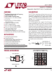
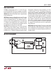
As shown in the Block Diagram, the LTC1799’s master
oscillator is controlled by the ratio of the voltage between
the V
+
and SET pins and the current entering the SET pin
(I
RES
). The voltage on the SET pin is forced to approximately
1.13V below V
+
by the PMOS transistor and its gate bias
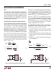
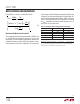
voltage. This voltage is accurate to ±7% at a particular
input current and supply voltage (see Figure 1). The ef-
fective input resistance is approximately 2k.
A resistor R
SET
, connected between the V
+
and SET pins,
“locks together” the voltage (V
+
– V
SET
) and current, I
RES
,
variation. This provides the LTC1799’s high precision. The
master oscillation frequency reduces to:
ƒ
MO
=10MHz •
10kΩ
R
SET
The LTC1799 is optimized for use with resistors between
10k and 200k, corresponding to master oscillator frequen-
cies between 0.5MHz and 10MHz. Accurate frequencies up
to 20MHz (R
SET
= 5k) are attainable if the supply voltage
is greater than 4V.
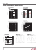
To extend the output frequency range, the master oscillator
signal may be divided by 1, 10 or 100 before driving OUT
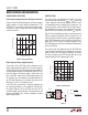
Figure 2. R
SET
vs Desired Output Frequency
(Pin 5). The divide-by value is determined by the state of
the DIV input (Pin 4). Tie DIV to GND or drive it below 0.5V
to select ÷1. This is the highest frequency range, with the
master output frequency passed directly to OUT. The DIV
pin may be floated or driven to midsupply to select ÷10,
the intermediate frequency range. The lowest frequency
range, ÷100, is selected by tying DIV to V
+
or driving it to
within 0.4V of V
+
. Figure 2 shows the relationship between
R
SET
, divider setting and output frequency, including the
overlapping frequency ranges near 100kHz and 1MHz.
The CMOS output driver has an on resistance that is typi-
cally less than 100Ω. In the ÷1 (high frequency) mode,
the rise and fall times are typically 7ns with a 5V supply
and 11ns with a 3V supply. These times maintain a clean
square wave at 10MHz (20MHz at 5V supply). In the ÷10
and ÷100 modes, where the output frequency is much lower,
slew rate control circuitry in the output driver increases
the rise/fall times to typically 14ns for a 5V supply and
19ns for a 3V supply. The reduced slew rate lowers EMI
(electromagnetic interference) and supply bounce.
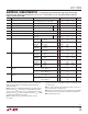
Figure 1. V
+
– V
SET
Variation with I
RES
I
RES
(µA)
1
0.8
V
RES
= V
+
– V
SET
1.2
1.3
1.4
10 100 1000
1799 F01
1.1
1.0
0.9
V
+
= 5V
V
+
= 3V
T
A
= 25°C
DESIRED OUTPUT FREQUENCY (Hz)
10
R
SET
(kΩ)
100
1k 100k 1M 10M
1799 F02
1
10k
1000
100M
÷100 ÷10 ÷1
MOST
ACCURATE
OPERATION