
Datasheet
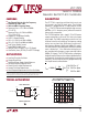


LTC1799
8
1799fc
applicaTions inForMaTion
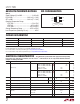
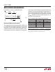
Figure 5. Supply Sensitivity
POWER SUPPLY REJECTION
Low Frequency Supply Rejection (Voltage Coefficient)
Figure 5 shows the output frequency sensitivity to power
supply voltage at several different temperatures. The
LTC1799 has a conservative guaranteed voltage coeffi-
cient of 0.1%/V but, as Figure 5 shows, the typical supply
sensitivity is lower.
START-UP TIME
The start-up time and settling time to within 1% of the
final value can be estimated by t
START
≅ R
SET
(2.8µs/kΩ)
+ 20µs. Note the start-up time depends on R
SET
and it
is independent from the setting of the divider pin. For
instance with R
SET
= 50k, the LTC1799 will settle with 1%
of its 200kHz final value (N = 10) in approximately 160µs.
Figure 6 shows start-up times for various R
SET
resistors.
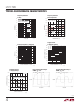
Figure 7 shows an application where a second set resistor
R
SET2
is connected in parallel with set resistor R
SET1
via
switch S1. When switch S1 is open, the output frequency
of the LTC1799 depends on the value of the resistor R
SET1
.
When switch S1 is closed, the output frequency of the
LTC1799 depends on the value of the parallel combination
of R
SET1
and R
SET2
.
The start-up time and settling time of the LTC1799 with
switch S1 open (or closed) is described by t
START
shown
above. Once the LTC1799 starts and settles, and switch
S1 closes (or opens), the LTC1799 will settle to its new
output frequency within approximately 25µs.
Figure 6. Start-Up Time
Figure 7
High Frequency Power Supply Rejection
The accuracy of the LTC1799 may be affected when its
power supply generates significant noise with frequency
contents in the vicinity of the programmed value of f
OSC
. If
a switching power supply is used to power up the LTC1799,
and if the ripple of the power supply is more than a few
tens of millivolts, make sure the switching frequency and
its harmonics are not related to the output frequency of
the LTC1799. Otherwise, the oscillator may show an ad-
ditional 0.1% to 0.2% of frequency error.
If the LTC1799 is powered by a switching regulator and
the switching frequency or its harmonics coincide with
the output frequency of the LTC1799, the jitter of the
oscillator output may be affected. This phenomenon will
become noticeable if the switching regulator exhibits
ripples beyond 30mV.
SUPPLY VOLTAGE (V)
2.5
–0.05
FREQUENCY DEVIATION (%)
0
0.05
0.10
0.15
3.0 3.5 4.0 4.5
1799 F05
5.0 5.5
85°C
–40°C
25°C
R
SET
= 31.6k
PIN 4 = FLOATING (÷10)
TIME AFTER POWER APPLIED (µs)
0
60
50
40
30
20
10
0
–10
300 500
1799 F06
100 200
400 600
FREQUENCY ERROR (%)
10k
31.6k
200k
T
A
= 25°C
V
+
= 5V
V
+
1
2
R
SET1
R
SET2
3
S1
5
V
+
1799 F07
4
GND
LTC1799
3V OR 5V
SET
OUT
DIV
÷10
÷100
÷1
f
OSC
= 10MHz •
OR
( )
10k
N • R
SET1
f
OSC
= 10MHz •
( )
10k
N • R
SET1
//R
SET2