
Datasheet

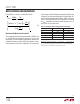

LTC1799
9
1799fc
applicaTions inForMaTion
Jitter
The typical jitter is listed in the Electrical Characteristics
and shown in the Typical Performance Characteristics.
These specifications assume that the capacitance on SET
(Pin 3) is limited to less than 10pF, as suggested in the Pin
Functions description. If this requirement is not met, the
jitter will increase. For more information, contact Linear
Technology Applications group.
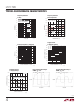
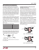
A Ground Referenced Voltage Controlled Oscillator
The LTC1799 output frequency can also be programmed by
steering current in or out of the SET pin, as conceptually
shown in Figure 8. This technique can degrade accuracy
as the ratio of (V
+
– V
SET
) / I
RES
is no longer uniquely
dependent of the value of R
SET
, as shown in the LTC1799
Block Diagram. This loss of accuracy will become notice-
able when the magnitude of I
PROG
is comparable to I
RES
.
The frequency variation of the LTC1799 is still monotonic.
Figure 9 shows how to implement the concept shown in
Figure 8 by connecting a second resistor, R
IN
, between
the SET pin and a ground referenced voltage source, V
IN
.
For a given power supply voltage in Figure 9, the output
frequency of the LTC1799 is a function of V
IN
, R
IN
, R
SET
and (V
+
– V
SET
) = V
RES
:
f
OSC
=
10MHz
N
•
10k
R
IN
R
SET
•
1+
V
IN
− V
+
( )
V
RES
•
1
1+
R
IN
R
SET
⎛
⎝
⎜
⎜
⎜
⎜
⎞
⎠
⎟
⎟
⎟
⎟
⎡
⎣
⎢
⎢
⎢
⎢
⎤
⎦
⎥
⎥
⎥
⎥
(1)
When V
IN
= V
+
, the output frequency of the LTC1799 as-
sumes the highest value and it is set by the parallel com-
bination of R
IN
and R
SET
. Also note, the output frequency,
f
OSC
, is independent of the value of V
RES
= (V
+
– V
SET
) so
the accuracy of f
OSC
is within the data sheet limits.
When V
IN
is less than V
+
, and especially when V
IN
ap-
proaches the ground potential, the oscillator frequency,
f
OSC
, assumes its lowest value and its accuracy is affected
by the change of V
RES
= (V
+
– V
SET
). At 25°C V
RES
varies
by ±8%, assuming the variation of V
+
is ±5%. The tem-
perature coefficient of V
RES
is 0.02%/°C.
By manipulating the algebraic relation for f
OSC
above, a
simple algorithm can be derived to set the values of external
resistors R
SET
and R
IN
, as shown in Figure 9.
1. Choose the desired value of the maximum oscillator
frequency, f
OSC(MAX)
, occurring at maximum input
voltage V
IN(MAX)
≤ V
+
.
2. Set the desired value of the minimum oscillator fre-
quency, f
OSC(MIN)
, occurring at minimum input voltage
V
IN(MIN)
≥ 0.
3. Choose V
RES
= 1.1 and calculate the ratio of R
IN
/R
SET
from the following:
R
IN
R
SET
=
V
IN(MAX)
− V
+
( )
−
f
OSC(MAX)
f
OSC(MIN)
⎛
⎝
⎜
⎞
⎠
⎟
V
IN(MIN)
− V
+
( )
V
RES
f
OSC(MAX)
( )
f
OSC(MIN)
−1
⎡
⎣
⎢
⎢
⎤
⎦
⎥
⎥
−1
(2)
Figure 9. Implementation of Concept Shown in Figure 8Figure 8. Concept for Programming via Current Steering
V
+
1
2
R
SET
I
PR
3
5
5V
V
+
1799 F08
4
GND
LTC1799
0.1µF
OPEN
SET
OUT
DIV
÷10
÷100
÷1
I
RES
V
+
1
2
R
SET
V
RES
R
IN
V
IN
3
5
5V
V
+
1799 F09
4
GND
LTC1799
0.1µF
f
OSC
OPEN
SET
OUT
DIV
÷10
÷100
÷1
+
–
+
–