
Datasheet

LTC1857/LTC1858/LTC1859
11
185789fa
APPLICATIONS INFORMATION
LT1227: 140MHz video current feedback amplifi er. 10mA
supply current. ±5V to ±15V supplies. Low noise and low
distortion.
LT1468/LT1469: Single and dual 90MHz, 16-bit accurate
op amp. Good AC/DC specs.
LT1677: Single, low noise op amp. Rail-to-rail input and
output. Up to ±15V supplies.
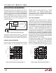
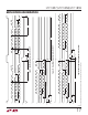
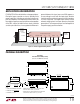
3000pF
1859 F02
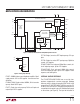
A
IN
+
A
IN
–
CH0
CH1
MUXOUT
+
MUXOUT
–
ADC
+
ADC
–
•
•
•
•
Figure 2. Analog Input Filtering
Figure 1. LTC1857/LTC1858/LTC1859 Simplifi ed Equivalent Circuit
LT1792: Single, low noise JFET input op amp, ±5V sup-
plies.
LT1793: Single, low noise JFET input op amp, 10pA bias
current, ±5V supplies.
LT1881/LT1882: Dual and quad, 200pA bias current, rail-
to-rail output op amps. Up to ±15V supplies.
LT1844/LT1885: Dual and quad, 400pA bias current,
rail-to-rail output op amps. Up to ±15V supplies. Faster
response and settling time.
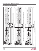
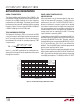
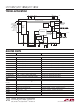
INTERNAL VOLTAGE REFERENCE
The LTC1857/LTC1858/LTC1859 have an on-chip, tem-
perature compensated, curvature corrected, bandgap
reference, which is factory trimmed to 2.50V. The full-scale
range of the LTC1857/LTC1858/LTC1859 is equal to ±5V,
0V to 5V, ±10V or 0V to 10V. The output of the reference is
connected to the input of a gain of 1.6384x buffer through
an 8k resistor (see Figure 3). The input to the buffer or
2.5V
REFERENCE
INTERNAL
CLOCK
1.6384X
4.096V
8k
AGND1
CONTROL
LOGIC
SERIAL I/O
INPUT MUX
AND
RANGE
SELECT
AGND3
AGND2REFCOMPV
REF
ADC
–
MUXOUT
+
MUXOUT
–
ADC
+
DGND
AV
DD
DV
DD
MUX ADDRESS AND RANGE
DATA OUT
CONVST
SDI
SCK
OV
DD
SDO
1859 BD
12-/14-/16-BIT
SAMPLING ADC
+
–
COM
CH7
CH1
•
•
•
CH0
BUSY
RD