
Datasheet


5
LTC1872B
OPERATIO
U
(Refer to Functional Diagram)
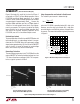
Figure 2 illustrates this result for the circuit of Figure 1
using both an LTC1872 in Burst Mode operation and an
LTC1872B (non-Burst Mode operation). At an output
current of 50mA, the Burst Mode operation part exhibits
an output ripple of approximately 80mV
P-P
, whereas the
non-Burst Mode operation part has an output ripple of
≈45mV
P-P
. At lower output current levels, the improve-
ment is even greater. This comes at a trade off of slightly
lower efficiency for the non-Burst Mode operation part.
Also notice the constant frequency operation of the
LTC1872B, even at 5% of maximum output current.
Undervoltage Lockout
To prevent operation of the N-channel MOSFET below safe
input voltage levels, an undervoltage lockout is incorpo-
rated into the LTC1872B. When the input supply voltage
drops below approximately 2.0V, the N-channel MOSFET
and all circuitry is turned off except the undervoltage
block, which draws only several microamperes.
Overvoltage Protection
The overvoltage comparator in the LTC1872B will turn the
external MOSFET off when the feedback voltage has risen
7.5% above the reference voltage of 0.8V. This compara-
tor has a typical hysteresis of 20mV.
Slope Compensation and Inductor’s Peak Current
The inductor’s peak current is determined by:
I
V
R
PK
ITH
SENSE
=
−
()
07
10
.
when the LTC1872B is operating below 40% duty cycle.
However, once the duty cycle exceeds 40%, slope com-
pensation begins and effectively reduces the peak induc-
tor current. The amount of reduction is given by the curves
in Figure 3.
Figure 2. Output Ripple Waveforms for the Circuit of Figure 1
V
IN
= 3.3V 5µs/DIV 1872B F02a
V
OUT
= 5V
I
OUT
= 50mA
20mV AC/DIV
V
IN
= 3.3V 5µs/DIV 1872B F02b
V
OUT
= 5V
I
OUT
= 50mA
20mV AC/DIV
Figure 3. Maximum Output Current vs Duty Cycle
DUTY CYCLE (%)
110
100
90
80
70
60
50
40
30
20
10
SF = I
OUT
/I
OUT(MAX)
(%)
1872B F03
0 70 80 90 1006010 20 30 40 50
I
RIPPLE
= 0.4I
PK
AT 5% DUTY CYCLE
I
RIPPLE
= 0.2I
PK
AT 5% DUTY CYCLE
V
IN
= 4.2V
(2a) V
OUT
Ripple for Figure 1 Circuit
Using LTC1872 Burst Mode Operation
(2b) V
OUT
Ripple for Figure 1 Circuit Using
LTC1872B Non-Burst Mode Operation