
Datasheet


12
LTC1878
Thermal Considerations
In most applications the LTC1878 does not dissipate
much heat due to its high efficiency. But, in applications
where the LTC1878 is running at high ambient tempera-
ture with low supply voltage and high duty cycles, such
as in dropout, the heat dissipated may exceed the maxi-
mum junction temperature of the part. If the junction
temperature reaches approximately 150°C, both power
switches will be turned off and the SW node will become
high impedance.
To avoid the LTC1878 from exceeding the maximum
junction temperature, the user will need to do some
thermal analysis. The goal of the thermal analysis is to
determine whether the power dissipated exceeds the
maximum junction temperature of the part. The tempera-
ture rise is given by:
T
R
= (P
D
)(θ
JA
)
where P
D
is the power dissipated by the regulator and q
JA
is the thermal resistance from the junction of the die to the
ambient temperature.
The junction temperature, T
J
, is given by:
T
J
= T
A
+ T
R
where T
A
is the ambient temperature.
As an example, consider the LTC1878 in dropout at an
input voltage of 3V, a load current of 500mA, and an
ambient temperature of 70°C. From the typical perfor-
mance graph of switch resistance, the R
DS(ON)
of the
P-channel switch at 70°C is approximately 0.7Ω. There-
fore, power dissipated by the part is:
P
D
= I
LOAD
2
• R
DS(ON)
= 0.175W
For the MSOP package, the θ
JA
is 150°C/W. Thus, the
junction temperature of the regulator is:
T
J
= 70°C + (0.175)(150) = 96°C
which is below the maximum junction temperature of
125°C.
Note that at higher supply voltages, the junction tempera-
ture is lower due to reduced switch resistance (R
DS(ON)
).
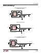
Checking Transient Response
The regulator loop response can be checked by looking at
the load transient response. Switching regulators take
several cycles to respond to a step in load current. When
a load step occurs, V
OUT
immediately shifts by an amount
equal to (∆I
LOAD
• ESR), where ESR is the effective series
resistance of C
OUT
. ∆I
LOAD
also begins to charge or
discharge C
OUT
, which generates a feedback error signal.
The regulator loop then acts to return V
OUT
to its steady-
state value. During this recovery time V
OUT
can be moni-
tored for overshoot or ringing that would indicate a stabil-
ity problem. The internal compensation provides adequate
compensation for most applications. But if additional
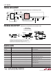
compensation is required, the I
TH
pin can be used for
external compensation using R
C
, C
C1
as shown in
Figure 7. (The 220pF capacitor, C
C2
, is typically needed for
noise decoupling.)
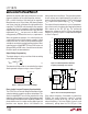
APPLICATIO S I FOR ATIO
WUUU
–
+
RUN
I
TH
V
FB
GND
PLL LPF
SYNC/MODE
SW
LTC1878
C
C2
C
C1
R
C
C
OUT
C
IN
1878 F07
L1
V
IN
BOLD LINES INDICATE
HIGH CURRENT PATHS
1
2
3
4
8
7
6
5
OPTIONAL
+
–
+
V
OUT
R2R1
V
IN
+
Figure 7. LTC1878 Layout Diagram