
Datasheet


23
LTC1966
sn1966 1966fas
IN1
V
DD
V
DD
V
SS
V
SS
R
SW
(TYP)
6k
C
EQ
2.5pF
(TYP)
C
EQ
2.5pF
(TYP)
I
IN1
IN2
I
IN2
1966 F21
R
SW
(TYP)
6k
IIN
VV
R
IIN
VV
R
RM
AVG
IN IN
EQ
AVG
IN IN
EQ
EQ
1
2
8
12
21
()
=
−
()
=
−
=
Ω
APPLICATIO S I FOR ATIO
WUUU
V
OUT
= (√(50mV AC)
2
+ (0.2mV DC)
2
) • 1.001 + 0.1mV
= 50.150mV
= 50mV + 0.301%
V
OUT
= (√(5mV AC)
2
+ (0.2mV DC)
2
) • 1.001 + 0.1mV
= 5.109mV
= 5mV + 2.18%
As can be seen, the gain term dominates with large inputs,
while the offset terms become significant with smaller
inputs. In fact, 5mV is the minimum RMS level needed to
keep the LTC1966 calculation core functioning normally,
so this represents the worst-case of usable input levels.
Using the worst-case values of the LTC1966 static errors,
the total conversion error is:
V
OUT
= (√(500mV AC)
2
+ (0.8mV DC)
2
) • 1.003 + 0.2mV
= 501.70mV
= 500mV + 0.340%
V
OUT
= (√(50mV AC)
2
+ (0.8mV DC)
2
) • 1.003 + 0.2mV
= 50.356mV
= 50mV + 0.713%
V
OUT
= (√(5mV AC)
2
+ (0.8mV DC)
2
) • 1.003 + 0.2mV
= 5.279mV
= 5mV + 5.57%
These static error terms are in addition to dynamic error
terms that depend on the input signal. See the Design
Cookbook for a discussion of the DC conversion error with
low frequency AC inputs. The LTC1966 bandwidth limita-
tions cause additional errors with high frequency inputs.
Another dynamic error is due to crest factor. The LTC1966
performance versus crest factor is shown in the Typical
Performance Characteristics.
Output Errors Versus Frequency
As mentioned in the design cookbook, the LTC1966 per-
forms very well with low frequency and very low frequency
inputs, provided a large enough averaging capacitor is
used.
However, the LTC1966 will have additional dynamic errors
as the input frequency is increased. The LTC1966 is de-
signed for high accuracy RMS-to-DC conversion of sig-
nals into the audible range. The input sampling amplifiers
have a –3dB frequency of 800kHz or so. However, the
switched capacitor circuitry samples the inputs at a mod-
est 100kHz nominal. The response versus frequency is
depicted in the Typical Performance Characteristics titled
Input Signal Bandwidth. Although there is a pattern to the
response versus frequency that repeats every sample fre-
quency, the errors are not overwhelming. This is because
LTC1966 RMS calculation is inherently wideband, operat-
ing properly with minimal oversampling, or even
undersampling, using several proprietary techniques to
exploit the fact that the RMS value of an aliased signal is
the same as the RMS value of the original signal. However,
a fundamental feature of the ∆Σ modulator is that sample
estimation noise is shaped such that minimal noise occurs
with input frequencies much less than the sampling fre-
quency, but such noise peaks when input frequency reaches
half the sampling frequency. Fortunately the LTC1966
output averaging filter greatly reduces this error, but the
RMS-to-DC topology frequency shifts the noise to low
(baseband) frequencies. So with input frequencies above
5kHz to 10kHz, the output will slowly wander around ±a
few percent.
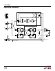
Input Impedance
The LTC1966 true RMS-to-DC converter utilizes a 2.5pF
capacitor to sample the input at a nominal 100kHz sample
frequency. This accounts for the 8MΩ input impedance.
See Figure 21 for the equivalent analog input circuit. Note
however, that the 8MΩ input impedance does not directly
affect the input sampling accuracy. For instance, if a 100k
source resistance is used to drive the LTC1966, the
sampling action of the input stage will drag down the
voltage seen at the input pins with small spikes at every
sample clock edge as the sample capacitor is connected to
be charged. The time constant of this combination is
Figure 21. LTC1966 Equivalent Analog Input Circuit