
Datasheet


15
LTC1967
1967f
Reducing Ripple with a Post Filter
The output ripple is always much larger than the DC error,
so filtering out the ripple can reduce the peak error
substantially, without the large settling time penalty of
simply increasing the averaging capacitor.
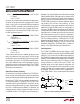
Figure 12 shows a basic 2nd order post filter, for a net 3rd
order filtering of the LTC1967 RMS calculation. It uses the
50kΩ output impedance of the LTC1967 as the first resis-
tor of a 3rd order Sallen-Key active-RC filter. This topology
features a buffered output, which can be desirable de-
pending on the application. However, there are disadvan-
tages to this topology, the first of which is that the op amp
input voltage and current errors directly degrade the effec-
tive LTC1967 V
OOS
. The table inset in Figure 12 shows
these errors for four of Linear Technology’s op amps.
A second disadvantage is that the op amp output has to
operate over the same range as the LTC1967 output, includ-
ing ground, which in single supply applications is the nega-
tive supply. Although the LTC1967 output will function fine
just millivolts from the rail, most op amp output stages (and
even some input stages) will not. There are at least two ways
to address this. First of all, the op amp can be operated split
supply if a negative supply is available. Just the op amp
would need to do so; the LTC1967 can remain single sup-
ply. A second way to address this issue is to create a signal
reference voltage a half volt or so above ground. This is most
attractive when the circuitry that follows has a differential
input, so that the tolerance of the signal reference is not a
APPLICATIO S I FOR ATIO
WUUU
concern. To do this, tie all three ground symbols shown in
Figure 12 to the signal reference, as well as to the differ-
ential return for the circuitry that follows.
Figure 13 shows an alternative 2nd order post filter, for a
net 3rd order filtering of the LTC1967 RMS calculation. It
also uses the 50kΩ output impedance of the LTC1967 as
the first resistor of a 3rd order active-RC filter, but this
topology filters without buffering so that the op amp DC
error characteristics do not affect the output. Although the
output impedance of the LTC1967 is increased from 50kΩ
to 168kΩ, this is not an issue with an extremely high input
impedance load, such as a dual-slope integrating ADC like
the ICL7106. And it allows a generic op amp to be used,
such as the SOT-23 one shown. Furthermore, it easily
works on a single supply rail by tying the noninverting
input of the op amp to a low noise reference as optionally
shown. This reference will not change the DC voltage at the
circuit output, although it does become the AC ground for
the filter, thus the (relatively) low noise requirement.
Step Responses with a Post Filter
B
oth of the post filters, shown in Figures 12 and 13, are
optimized for additional filtering with clean step re-
sponses. The 50kΩ output impedance of the LTC1967
working into a 2.2µF capacitor forms a 1st order LPF with
a –3dB frequency of ~1.45Hz. The two filters have 2.2µF
at the LTC1967 output for easy comparison with a
2.2µF-only case, and both have the same relative Bessel-
like shape. However, because of the topological differ-
ences of pole placements between the various compo-
nents within the two filters, the net effective bandwidth
for Figure 12 is slightly higher (≈1.2 • 1.45 ≈ 1.7Hz) than
with 2.2µF alone, while the bandwidth for Figure 13 is
Figure 13. DC Accurate Post Filter
Figure 12. Buffered Post Filter
LTC1967 C
AVE
2.2µF
5
6
R1
23.2k
–
+
R2
102k
R
B
C2
0.22µF
C1
2.2µF
LT1880
1967 F12
OP AMP
LTC1967 V
OOS
V
IOS
I
B/OS
• R
TOTAL OFFSET
R
B
VALUE
I
SQ
LT1494
±375µV
±43µV
±918µV
174k
1µA
LT1880
±150µV
±195µV
±845µV
SHORT
1.2mA
LT1077
±60µV
±329µV
±889µV
174k
48µA
LTC2054
±3µV
±52µV
±555µV
SHORT
150µA
±500µV
LTC1967 C
AVE
2.2µF
5
6
OTHER
REF VOLTAGE,
SEE TEXT
R1
118k
–
+
R2
402k
C1
0.47µF
C2
0.47µF
LT1782
1067 F13