
Datasheet


10
LTC1968
1968f
Because this peak has energy (proportional to voltage
squared) that is 16 times (4
2
) the energy of the RMS value,
the peak is necessarily present for at most 6.25% (1/16)
of the time.
The LTC1968 performs very well with crest factors of 4 or
less and will respond with reduced accuracy to signals
with higher crest factors. The high performance with crest
factors less than 4 is directly attributable to the high
linearity throughout the LTC1968.
DESIGN COOKBOOK
The LTC1968 RMS-to-DC converter makes it easy to
implement a rather quirky function. For many applications
all that will be needed is a single capacitor for averaging,
appropriate selection of the I/O connections and power
supply bypassing. Of course, the LTC1968 also requires
power. A wide variety of power supply configurations are
shown in the Typical Applications section towards the end
of this data sheet.
Capacitor Value Selection
The RMS or root-mean-squared value of a signal,
the root
of the mean of the square
, cannot be computed without
some averaging to obtain the
mean
function. The LTC1968
true RMS-to-DC converter utilizes a single capacitor on
the output to do the low frequency averaging required for
RMS-to-DC conversion. To give an accurate measure of a
dynamic waveform, the averaging must take place over a
sufficiently long interval to average, rather than track, the
lowest frequency signals of interest. For a single averaging
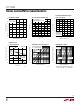
capacitor, the accuracy at low frequencies is depicted in
Figure 6.
Figure 6 depicts the so-called “DC error” that results at a
given combination of input frequency and filter capacitor
values
2
. It is appropriate for most applications, in which
the output is fed to a circuit with an inherently band-limited
frequency response, such as a dual slope/integrating A/D
converter, a ∆Σ A/D converter or even a mechanical analog
meter.
However, if the output is examined on an oscilloscope with
a very low frequency input, the incomplete averaging will
be seen, and this ripple will be larger than the error
depicted in Figure 6. Such an output is depicted in
Figure 7. The ripple is at twice the frequency of the input
APPLICATIO S I FOR ATIO
WUUU
Figure 6. DC Error vs Input Frequency
Figure 7. Output Ripple Exceeds DC Error
TIME
OUTPUT
1968 F07
DC
ERROR
(0.05%)
IDEAL
OUTPUT
DC
AVERAGE
OF ACTUAL
OUTPUT
PEAK
RIPPLE
(5%)
ACTUAL OUTPUT
WITH RIPPLE
f = 2 × f
INPUT
PEAK
ERROR =
DC ERROR +
PEAK RIPPLE
(5.05%)
2
This frequency-dependent error is in additon to the static errors that affect all readings and are
therefore easy to trim or calibrate out. The “Error Analyses” section to follow discusses the effect
of static error terms.
INPUT FREQUENCY (Hz)
1
–2.0
DC ERROR (%)
–1.6
–1.2
–0.8
–0.4
10 100
1968 F06
0
–1.8
–1.4
–1.0
–0.6
–0.2
C = 0.22µFC = 0.47µFC = 1µF
C = 10µF
C = 2.2µF
C = 22µF
C = 47µF
C = 4.7µF