
Datasheet


LTC1992 Family
24
1992fb
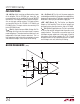
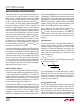
PIN FUNCTIONS
–IN, +IN (Pins 1, 8): Inverting and Noninverting Inputs
of the Amplifier. For the LTC1992 part, these pins are
connected directly to the amplifier’s P-channel MOSFET
input devices. The fixed gain LTC1992-X parts have preci-
sion, on-chip gain setting resistors. The input resistors
are nominally 30k for the LTC1992-1, LTC1992-2 and
LTC1992-5 parts. The input resistors are nominally 15k
for the LTC1992-10 part.
V
OCM
(Pin 2): Output Common Mode Voltage Set Pin.
The voltage on this pin sets the output signal’s common
mode voltage level. The output common mode level is set
independent of the input common mode level. This is a
high impedance input and must be connected to a known
and controlled voltage. It must never be left floating.
+V
S
, –V
S
(Pins 3, 6): The +V
S
and –V
S
power supply pins
should be bypassed with 0.1μF capacitors to an adequate ana-
log ground or ground plane. The bypass capacitors should
be located as closely as possible to the supply pins.
+OUT, –OUT (Pins 4, 5): The Positive and Negative
Outputs of the Amplifier. These rail-to-rail outputs are
designed to drive capacitive loads as high as 10,000pF.
V
MID
(Pin 7): Mid-Supply Reference. This pin is connected
to an on-chip resistive voltage divider to provide a mid-
supply reference. This provides a convenient way to set
the output common mode level at half-supply. If used for
this purpose, Pin 2 will be shorted to Pin 7, Pin 7 should
be bypassed with a 0.1μF capacitor to ground. If this refer-
ence voltage is not used, leave the pin floating.
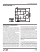
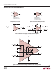
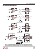
BLOCK DIAGRAMS
(1992)
+
–
1
7
2
6
3
8
5
4
+
–
200k
200k
+V
S
–V
S
V
+
V
–
30k
30k
A1
+
+
+
–
A2
+OUT
1992 BD
–IN
V
MID
V
OCM
+IN
–OUT
+V
S
–V
S
+V
S
–V
S