LTC1992 Family Low Power, Fully Differential Input/Output Amplifier/Driver Family FEATURES DESCRIPTION n The LTC®1992 product family consists of five fully differential, low power amplifiers. The LTC1992 is an unconstrained fully differential amplifier. The LTC1992-1, LTC1992-2, LTC1992-5 and LTC1992-10 are fixed gain blocks (with gains of 1, 2, 5 and 10 respectively) featuring precision on-chip resistors for accurate and ultrastable gain.
LTC1992 Family ABSOLUTE MAXIMUM RATINGS (Note 1) Total Supply Voltage (+VS to –VS) .............................12V Maximum Voltage on any Pin ................ (–VS – 0.3V) ≤ VPIN ≤ (+VS + 0.3V) Output Short-Circuit Duration (Note 3) ............ Indefinite Operating Temperature Range (Note 5) LTC1992CMS8/LTC1992-XCMS8/ LTC1992IMS8/LTC1992-XIMS8 ...........–40°C to 85°C LTC1992HMS8/LTC1992-XHMS8 ...... –40°C to 125°C Specified Temperature Range (Note 6) LTC1992CMS8/LTC1992-XCMS8 .............
LTC1992 Family ELECTRICAL CHARACTERISTICS The l denotes the specifications which apply over the full operating temperature range, otherwise specifications are at TA = 25°C. +VS = 5V, –VS = 0V, VINCM = VOUTCM = VOCM = 2.5V, unless otherwise noted. VOCM is the voltage on the VOCM pin. VOUTCM is defined as (+VOUT + –VOUT)/2. VINCM is defined as (+VIN + –VIN)/2. VINDIFF is defined as (+VIN – –VIN). VOUTDIFF is defined as (+VOUT – –VOUT). Specifications applicable to all parts in the LTC1992 family.
LTC1992 Family ELECTRICAL CHARACTERISTICS The l denotes the specifications which apply over the full operating temperature range, otherwise specifications are at TA = 25°C. +VS = 5V, –VS = 0V, VINCM = VOUTCM = VOCM = 2.5V, unless otherwise noted. VOCM is the voltage on the VOCM pin. VOUTCM is defined as (+VOUT + –VOUT)/2. VINCM is defined as (+VIN + –VIN)/2. VINDIFF is defined as (+VIN – –VIN). VOUTDIFF is defined as (+VOUT – –VOUT). Specifications applicable to all parts in the LTC1992 family.
LTC1992 Family ELECTRICAL CHARACTERISTICS The l denotes the specifications which apply over the full operating temperature range, otherwise specifications are at TA = 25°C. +VS = 5V, –VS = 0V, VINCM = VOUTCM = VOCM = 2.5V, unless otherwise noted. VOCM is the voltage on the VOCM pin. VOUTCM is defined as (+VOUT + –VOUT)/2. VINCM is defined as (+VIN + –VIN)/2. VINDIFF is defined as (+VIN – –VIN). VOUTDIFF is defined as (+VOUT – –VOUT). Typical values are at TA = 25°C.
LTC1992 Family ELECTRICAL CHARACTERISTICS The l denotes the specifications which apply over the full operating temperature range, otherwise specifications are at TA = 25°C. +VS = 5V, –VS = 0V, VINCM = VOUTCM = VOCM = 2.5V, unless otherwise noted. VOCM is the voltage on the VOCM pin. VOUTCM is defined as (+VOUT + –VOUT)/2. VINCM is defined as (+VIN + –VIN)/2. VINDIFF is defined as (+VIN – –VIN). VOUTDIFF is defined as (+VOUT – –VOUT). Typical values are at TA = 25°C.
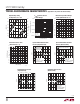
LTC1992 Family TYPICAL PERFORMANCE CHARACTERISTICS Differential Input Offset Voltage vs Temperature (Note 7) 0.6 1.0 DIFFERENTIAL VOS (mV) SUPPLY CURRENT (mA) 0.4 85°C 25°C 0.7 0.6 –40°C 0.5 0.4 0.3 0 VS = ±1.35V VS = ±2.5V –0.2 –0.4 VS = ±5V –0.6 0.1 0 1 2 3 4 5 6 7 8 TOTAL SUPPLY VOLTAGE (V) 9 –0.
LTC1992 Family TYPICAL PERFORMANCE CHARACTERISTICS Applicable to all parts in the LTC1992 family. VOCM Input Bias Current vs VOCM Voltage Output Voltage Swing vs Output Load, VS = ±5V 5.0 Differential Input Offset Voltage vs Time (Normalized to t = 0) 10E-9 –3.8 100 TEMP = 35°C –4.0 –40°C –4.2 25°C 4.7 –4.4 125°C 85°C 85°C 4.6 125°C –4.6 25°C 4.5 –4.8 –40°C 4.4 5 10 0 –20 –15 –10 –5 LOAD CURRENT (mA) –SWING (V) –5.
LTC1992 Family TYPICAL PERFORMANCE CHARACTERISTICS Single-Ended Input Differential Gain vs Frequency, VS = ±2.5V CLOAD = 10000pF CLOAD = 5000pF CLOAD = 1000pF CLOAD = 500pF CLOAD = 100pF CLOAD = 50pF CLOAD = 10pF 100 1000 FREQUENCY (kHz) 12 6 0 –6 –12 –18 –24 –30 –36 –42 –48 –54 –60 –66 –20 CLOAD = 10000pF CLOAD = 5000pF CLOAD = 1000pF CLOAD = 500pF CLOAD = 100pF CLOAD = 50pF CLOAD = 10pF 10 10000 –140 –160 –180 100 1000 FREQUENCY (kHz) 10 10000 –40°C 125°C 85°C –1.0 –1.5 2.0 1.0 0.
LTC1992 Family TYPICAL PERFORMANCE CHARACTERISTICS ± 0V VOUTDIFF (1V/DIV) +VS = 2.5V –VS = –2.5V VOCM = 0V +VIN = ±1.5V –VIN = 1.5V CLOAD = 0pF GAIN = 1 Differential Input Large-Signal Step Response +VS = 2.5V –VS = –2.5V VOCM = 0V +VIN = ±1.5V –VIN = 1.5V GAIN = 1 ± VOUTDIFF (1V/DIV) Differential Input Large-Signal Step Response Applicable to the LTC1992 only. 0V CLOAD = 10000pF CLOAD = 1000pF 2μs/DIV 20μs/DIV 1992 G26 +VS = 5V –VS = 0V VOCM = 2.
LTC1992 Family TYPICAL PERFORMANCE CHARACTERISTICS Applicable to the LTC1992 only. Single-Ended Input Small-Signal Step Response Single-Ended Input Small-Signal Step Response VOUTDIFF (50mV/DIV) VOUTDIFF (50mV/DIV) CLOAD = 10000pF CLOAD = 1000pF 2.5V +VS = 5V –VS = 0V VOCM = 2.5V +VIN = 0V TO 200mV –VIN = 100mV CLOAD = 0pF GAIN = 1 1μs/DIV 2.5V +VS = 5V –VS = 0V VOCM = 2.
LTC1992 Family TYPICAL PERFORMANCE CHARACTERISTICS Single-Ended Input Differential Gain vs Frequency, VS = ±2.
LTC1992 Family TYPICAL PERFORMANCE CHARACTERISTICS Common Mode Rejection Ratio vs Frequency 100 +VS = 2.5V –VS = –2.5V VOCM = 0V +VIN = ±1.5V –VIN = 1.5V 90 80 70 CMRR (dB) ± 0V VOUTDIFF (1V/DIV) +VS = 2.5V –VS = –2.5V VOCM = 0V +VIN = ±1.5V –VIN = 1.5V CLOAD = 0pF Differential Input Large-Signal Step Response ± VOUTDIFF (1V/DIV) Differential Input Large-Signal Step Response Applicable to the LTC1992-1 only.
LTC1992 Family TYPICAL PERFORMANCE CHARACTERISTICS Single-Ended Input Small-Signal Step Response Applicable to the LTC1992-1 only. Single-Ended Input Small-Signal Step Response Differential Noise Voltage Density vs Frequency 1000 2.5V +VS = 5V –VS = 0V VOCM = 2.5V +VIN = 0V TO 200mV –VIN = 100mV CLOAD = 0pF 1μs/DIV INPUT REFERRED NOISE (nV√Hz) VOUTDIFF (50mV/DIV) VOUTDIFF (50mV/DIV) CLOAD = 10000pF CLOAD = 1000pF 2.5V +VS = 5V –VS = 0V VOCM = 2.
LTC1992 Family TYPICAL PERFORMANCE CHARACTERISTICS Single-Ended Input Differential Gain vs Frequency, VS = ±2.5V CLOAD = 10000pF CLOAD = 5000pF CLOAD = 1000pF CLOAD = 500pF CLOAD = 100pF CLOAD = 50pF CLOAD = 10pF 10 100 1000 FREQUENCY (kHz) 10000 Differential Phase Response vs Frequency 0 18 12 6 0 –6 –12 –18 –24 –30 –36 –42 –48 –54 –60 –66 10 –20 –40 PHASE (DEG) GAIN (dB) GAIN (dB) Differential Input Differential Gain vs Frequency, VS = ±2.
LTC1992 Family TYPICAL PERFORMANCE CHARACTERISTICS Differential Input Large-Signal Step Response 90 80 70 CMRR (dB) VOUTDIFF (1V/DIV) 100 +VS = 2.5V –VS = –2.5V VOCM = 0V +VIN = ±750mV –VIN = 750mV ± 0V Common Mode Rejection Ratio vs Frequency (Note 7) ± VOUTDIFF (1V/DIV) Differential Input Large-Signal Step Response +VS = 2.5V –VS = –2.5V VOCM = 0V +VIN = ±750mV –VIN = 750mV CLOAD = 0pF Applicable to the LTC1992-2 only.
LTC1992 Family TYPICAL PERFORMANCE CHARACTERISTICS Single-Ended Input Small-Signal Step Response Applicable to the LTC1992-2 only. Single-Ended Input Small-Signal Step Response Differential Noise Voltage Density vs Frequency 1000 +VS = 5V –VS = 0V VOCM = 2.5V +VIN = 0V TO 100mV –VIN = 50mV CLOAD = 0pF 2μs/DIV INPUT REFERRED NOISE (nV√Hz) VOUTDIFF (50mV/DIV) 2.5V 2.5V +VS = 5V –VS = 0V VOCM = 2.
LTC1992 Family TYPICAL PERFORMANCE CHARACTERISTICS Single-Ended Input Differential Gain vs Frequency, VS = ±2.
LTC1992 Family TYPICAL PERFORMANCE CHARACTERISTICS Common Mode Rejection Ratio vs Frequency (Note 7) 100 +VS = 2.5V –VS = –2.5V VOCM = 0V +VIN = ± 300mV –VIN = 300mV 90 80 70 CMRR (dB) ± 0V VOUTDIFF (1V/DIV) +VS = 2.5V –VS = –2.5V VOCM = 0V +VIN = ± 300mV –VIN = 300mV CLOAD = 0pF Differential Input Large-Signal Step Response ± VOUTDIFF (1V/DIV) Differential Input Large-Signal Step Response Applicable to the LTC1992-5 only.
LTC1992 Family TYPICAL PERFORMANCE CHARACTERISTICS Single-Ended Input Small-Signal Step Response Differential Noise Voltage Density vs Frequency VOUTDIFF (50mV/DIV) VOUTDIFF (50mV/DIV) CLOAD = 10000pF CLOAD = 1000pF 2.5V +VS = 5V –VS = 0V VOCM = 2.5V +VIN = 0V TO 40mV –VIN = 20mV CLOAD = 0pF 5μs/DIV 2.5V +VS = 5V –VS = 0V VOCM = 2.
LTC1992 Family TYPICAL PERFORMANCE CHARACTERISTICS Single-Ended Input Differential Gain vs Frequency, VS = ±2.5V Differential Input Differential Gain vs Frequency, VS = ±2.
LTC1992 Family TYPICAL PERFORMANCE CHARACTERISTICS Common Mode Rejection Ratio vs Frequency (Note 7) 100 +VS = 2.5V –VS = –2.5V VOCM = 0V +VIN = ±150mV –VIN = 150mV 90 80 70 CMRR (dB) ± 0V VOUTDIFF (1V/DIV) +VS = 2.5V –VS = –2.5V VOCM = 0V +VIN = ±150mV –VIN = 150mV CLOAD = 0pF Differential Input Large-Signal Step Response ± VOUTDIFF (1V/DIV) Differential Input Large-Signal Step Response Applicable to the LTC1992-10 only.
LTC1992 Family TYPICAL PERFORMANCE CHARACTERISTICS Single-Ended Input Small-Signal Step Response Differential Noise Voltage Density vs Frequency VOUTDIFF (50mV/DIV) 2.5V +VS = 5V –VS = 0V VOCM = 2.5V +VIN = 0V TO 20mV –VIN = 10mV CLOAD = 0pF 10μs/DIV 2.5V +VS = 5V –VS = 0V VOCM = 2.
LTC1992 Family PIN FUNCTIONS –IN, +IN (Pins 1, 8): Inverting and Noninverting Inputs of the Amplifier. For the LTC1992 part, these pins are connected directly to the amplifier’s P-channel MOSFET input devices. The fixed gain LTC1992-X parts have precision, on-chip gain setting resistors. The input resistors are nominally 30k for the LTC1992-1, LTC1992-2 and LTC1992-5 parts. The input resistors are nominally 15k for the LTC1992-10 part.
LTC1992 Family BLOCK DIAGRAMS (1992-X) +VS 3 +VS –IN RIN RFB 1 200k –VS VMID +VS RIN PART LTC1992-1 LTC1992-2 LTC1992-5 LTC1992-10 RIN 4 +OUT + – 5 –OUT 7 200k +IN – + RFB 8 RFB 30k 30k 30k 60k 30k 150k 15k 150k –VS 6 –VS 2 VOCM 1992-X BD APPLICATIONS INFORMATION Theory of Operation The LTC1992 family consists of five fully differential, low power amplifiers. The LTC1992 is an unconstrained fully differential amplifier.
LTC1992 Family APPLICATIONS INFORMATION Op Amp –IN Fully Differential Amplifier – –IN LTC1992 AO +IN VOCM OUT + +IN • DIFFERENTIAL INPUT • HIGH OPEN-LOOP GAIN • SINGLE-ENDED OUTPUT • • • • Op Amp with Negative Feedback – + + – RIN Fully Differential Amplifier with Negative Feedback RFB RIN – – –VIN LTC1992 + +VOUT VOCM –VOUT VOCM LTC1992 VOUT RIN + –OUT DIFFERENTIAL INPUT HIGH OPEN-LOOP GAIN DIFFERENTIAL OUTPUT VOCM INPUT SETS OUTPUT COMMON MODE LEVEL RFB VIN +OUT LTC1992 AO
LTC1992 Family APPLICATIONS INFORMATION negative feedback and using an op amp’s differential input to create the servo’s summing junction. One servo controls the signal gain path. The differential input of op amp A1 creates the summing junction of this servo. Any voltage present at the input of A1 is amplified (by the op amp’s large open-loop gain), sent to the summing blocks and then onto the outputs.
LTC1992 Family APPLICATIONS INFORMATION RFB RIN A INM 2AVP-P –VIN –A VINDIFF 4AVP-PDIFF RIN 2AVP-P +VIN –A + +VOUT VOCM LTC1992 VOCM VINCM A – INP B –B 2BVP-P VOUTDIFF 4BVP-PDIFF VOUTCM + – –VOUT B –B 2BVP-P RFB 1992 F03 DIFFERENTIAL = V INDIFF = +VIN – –VIN INPUT VOLTAGE DIFFERENTIAL = VOUTDIFF = +VOUT – –VOUT OUTPUT VOLTAGE +VIN + –VIN INPUT COMMON = V INCM = 2 MODE VOLTAGE +VOUT + –VOUT OUTPUT COMMON = V OUTCM = 2 MODE VOLTAGE ( ( ) ) +VOUT = +VIN – –VIN • 1 RFB • + VOCM 2 R
LTC1992 Family APPLICATIONS INFORMATION Gain Block RFB RIN RIN – VIN RFB VOUT + + – +VIN R GAIN = FB RIN CIN AC Coupled Gain Block – RFB RIN VOUT CIN + – +VIN RIN –VOUT RFB Single Pole Lowpass Filter C RFB RFB RIN – VIN +VOUT VOCM LTC1992 RIN S H(S) = HO • S + WP R 1 HO = FB ; WP = RIN RIN • CIN C + – –VIN + –VOUT RFB CIN RIN VIN +VOUT VOCM LTC1992 RIN RFB + – –VIN VOUT + + – +VIN WP S + WP RFB RFB 1 ;W = RIN P RFB • C C H(S) = HO • 3-Pole Lowpass Filter
LTC1992 Family APPLICATIONS INFORMATION The VOCM input pin has a very high input impedance and is easily driven by even the weakest of sources. Many ADCs provide a voltage reference output that defines either its common mode level or its full-scale level. Apply the ADC’s reference potential either directly to the VOCM pin or through a resistive voltage divider depending on the reference voltage’s definition. When controlling the VOCM pin by a high impedance source, connect a bypass capacitor (1000pF to 0.
LTC1992 Family APPLICATIONS INFORMATION Typical Performance plots for small-signal step response, large-signal step response and gain over frequency to appraise the effects of capacitive loading. While the consequences are minor in most instances, consider these effects when designing application circuits with large capacitive loads. Input Signal Amplitude Considerations For application circuits to operate correctly, the amplifier must be in its linear operating range.
LTC1992 Family APPLICATIONS INFORMATION Differential Input Signals RFB A 2AVP-P –VIN –A VINDIFF 4AVP-PDIFF INM RIN NODE – RIN A 2AVP-P +VIN –A –B 2BVP-P VOUTDIFF 4BVP-PDIFF VOUTCM + – INP NODE B +VOUT VOCM LTC1992 VOCM VINCM + –VOUT B –B 2BVP-P R G = FB RIN RFB INPUT COMMON MODE LIMITS A. CALCULATE VINCM MINIMUM AND MAXIMUM GIVEN RIN, RFB AND VOCM 1 VINCM(MAX) = (+VS – 1.3V) + (+VS – 1.3V – VOCM) G 1 VINCM(MIN) = (–VS – 0.1V) + (–VS – 0.1V – VOCM) G OR B.
LTC1992 Family APPLICATIONS INFORMATION Table 1. Input Signal Limitations for Some Common Applications Differential Input Signal, VOCM at Mid-Supply. (VINCM must be within the Min and Max table values and VINDIFF must be less than the table value) +VS (V) –VS (V) GAIN (V/V) VOCM (V) VINCM(MAX) (V) VINCM(MIN) (V) VINDIFF(MAX) (VP-PDIFF) VOUTDIFF(MAX) (VP-PDIFF) 2.7 0 1 1.35 1.450 –1.550 5.40 5.40 2.7 0 2 1.35 1.425 –0.825 2.70 5.40 2.7 0 5 1.35 1.410 –0.390 1.08 5.40 2.
LTC1992 Family APPLICATIONS INFORMATION Table 1. Input Signal Limitations for Some Common Applications Mid-Supply Referenced Single-Ended Input Signal, VOCM at Mid-Supply. (The VINSIG Min and Max values listed account for both the input common mode limits and the output clipping) +VS (V) –VS (V) GAIN (V/V) VOCM (V) VINREF (V) VINSIG(MAX) (V) VINSIG(MIN) (V) VINSIGP-P(MAX) (VP-P AROUND VINREF) VOUTDIFF(MAX) (VP-PDIFF) 2.7 0 1 1.35 1.35 1.550 –1.350 0.40 0.40 2.7 0 2 1.35 1.35 1.500 0.
LTC1992 Family APPLICATIONS INFORMATION Table 1. Input Signal Limitations for Some Common Applications Single Supply Ground Referenced Single-Ended Input Signal, VOCM at Mid-Supply. (The VINSIG Min and Max values listed account for both the input common mode limits and the output clipping) +VS (V) –VS (V) GAIN (V/V) VOCM (V) VINREF (V) VINSIG(MAX) (V) VINSIG(MIN) (V) VINSIGP-P(MAX) (VP-P AROUND VINREF) VOUTDIFF(MAX) (VP-PDIFF) 2.7 0 1 1.35 0 2.700 –2.700 5.40 5.40 2.7 0 2 1.35 0 1.
LTC1992 Family APPLICATIONS INFORMATION RFB2 RIN2 VINDIFF +VIN – –VIN + – –VIN VOCM RIN1 +VOUT + – +VIN VOUTDIFF +VOUT – –VOUT VOCM LTC1992 –VOUT RFB1 VOUTDIFF = 2[+VIN • (1 – B1) – (–VIN) • (1 – B2)] + 2VOSDIFF + 2VOUTCM (B1 – B2) B1 + B2 WHERE: B1 = RIN1 RIN2 ; B2 = RIN1 + RFB1 RIN2 + RFB2 ; VOSDIFF = AMPLIFIER INPUT REFERRED OFFSET VOLTAGE VOUTCM = KCM • VOCM + VOSCM 0.999 < KCM < 1.
LTC1992 Family APPLICATIONS INFORMATION – + VOCM VIN +VOUT VOUTDIFF = 2(+VIN – VOCM) –VOUT SETTING VOCM = 0V VOCM LTC1992 + – VOUTDIFF = 2VIN RIN RFB – + VOCM VIN VOCM ( VOUTDIFF = 2 +VIN 1 – VOCM B ) ;B= RIN RIN + RFB VOCM LTC1992 + – –VOUT – + +VOUT SETTING VOCM = 0V RFB 1 VOUTDIFF = 2VIN B = 2VIN 1 + R IN () ( ( VOUTDIFF = 2 +VIN 1–B + VOCM B ) ) ;B= RIN RIN + RFB VOCM LTC1992 RIN VIN +VOUT + – –VOUT RFB SETTING VOCM = 0V RFB 1–B VOUTDIFF = 2VIN B = 2VIN R IN ( ) ( )
LTC1992 Family TYPICAL APPLICATIONS Interfacing a Bipolar, Ground Referenced, Single-Ended Signal to a Unipolar Single Supply, Differential Input ADC (VIN = 0V Gives a Digital Mid-Scale Code) 5V 1μF 0.1μF 40k 10k 13.3k 3 10k 1 7 – + VMID 2 2.5V VIN –2.5V 10k VOCM 8 0V 2 +IN 100pF LTC1992 + – 5V 100Ω 4 1 8 VREF VCC SCK LTC1864 100Ω 3 5 CONV –IN 6 5 SERIAL DATA LINK GND 6 13.3k SDO 7 4 1992 TA02a 10k 0.1μF 40k Compact, Unipolar Serial Data Conversion 5V 1μF 3 0.
LTC1992 Family TYPICAL APPLICATIONS Single-Ended to Differential Conversion Driving an ADC 10μF 2.2μF 10Ω + 3 VREF 5V 10μF + 36 AVDD 5V 35 9 AVDD 10μF + 10 DVDD DGND SHDN 33 LTC1603 4 REFCOMP 5V + 7.5k 2.5V REF 1.75X 4.375V CONTROL LOGIC AND TIMING 47μF 0.1μF 100Ω LTC1992-1 VOCM + – 6 + 1 AIN 2 5 OGND 28 + 100pF AIN– – 100Ω 16-BIT SAMPLING ADC AGND 5 0.
LTC1992 Family PACKAGE DESCRIPTION MS8 Package 8-Lead Plastic MSOP (Reference LTC DWG # 05-08-1660 Rev F) 3.00 p 0.102 (.118 p .004) (NOTE 3) 0.889 p 0.127 (.035 p .005) 0.254 (.010) 8 7 6 5 3.00 p 0.102 (.118 p .004) (NOTE 4) 4.90 p 0.152 (.193 p .006) DETAIL “A” 0.52 (.0205) REF 0o – 6o TYP GAUGE PLANE 5.23 (.206) MIN 1 3.20 – 3.45 (.126 – .136) 0.53 p 0.152 (.021 p .006) DETAIL “A” 0.42 p 0.038 (.0165 p .0015) TYP 0.65 (.0256) BSC 1.10 (.043) MAX 2 3 4 0.86 (.034) REF 0.18 (.
LTC1992 Family REVISION HISTORY REV DATE DESCRIPTION PAGE NUMBER A 7/10 Updated Part Markings 2 B 6/11 Revised Features 1 Updated to Specified Temperature Range in Absolute Maximum Ratings and Order Information 2 Revised Block Diagram 24 Revised subtitle in Figure 5 of Applications Information section 32 1992fb Information furnished by Linear Technology Corporation is believed to be accurate and reliable. However, no responsibility is assumed for its use.
LTC1992 Family TYPICAL APPLICATION Balanced Frequency Converter (Suitable for Frequencies up to 50kHz) 60kHz LOW PASS FILTER SAMPLER 2kHz LOWPASS FILTER 5V 0.1μF 9.53k 0.1μF 0.1μF 120pF 9.53k 8.87k 7 BNC 9.53k VINP 3 1 330pF 2 8.87k 8 75k 4 – + VMID 4 7 6 60.4k 1 7 13 1/2 LTC1043 + – 5 12 37.4k 180pF 2 60.4k 8 14 16 120pF 11 37.4k 8 LTC1992 VOCM 390pF V+ 9.53k 3 – + VMID VOCM + – 390pF 17 0.1μF 0.